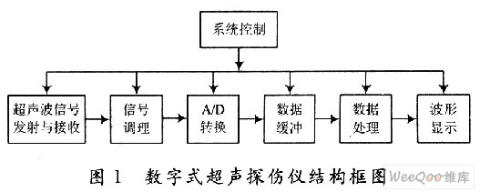
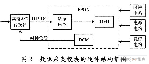
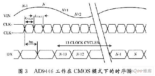
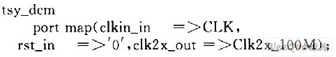
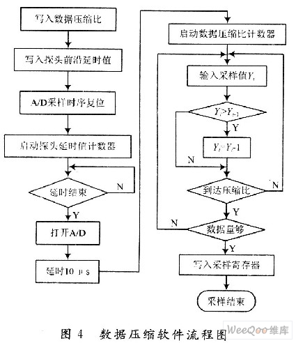
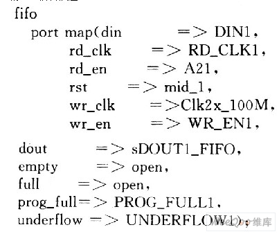
Technology of high-speed data acquisition module in digital ultrasonic flaw detector Due to its advantages of strong penetrating power and high detection sensitivity, ultrasonic testing plays an extensive role in aerospace, metallurgical shipbuilding, petrochemical industry, railways and other fields. Generally, ultrasonic flaw detectors that use ultrasonic non-destructive testing technology are divided into analog and digital. With the development of computer technology, microelectronic technology and digital signal processing technology, traditional analog ultrasonic flaw detectors are gradually being used by advanced digital functions. Replaced by ultrasonic flaw detector. The echo signal of the ultrasonic wave is a high-frequency signal, and its center frequency is up to 20 MHz or more. The frequency of the echo signal in a commonly used ultrasonic probe is generally 2.5 to 10 MHz. To digitize such a high-frequency signal, the system The analog / digital conversion circuit puts forward very high requirements. According to Shannon sampling theorem and Nyquist sampling criterion, in an ideal data acquisition system, in order to reproduce the input signal without distortion, the sampling frequency is at least twice the highest frequency of the input signal. In actual use, in order to ensure the accuracy of data collection, the number of samples in each input signal cycle should be increased, generally 7 to 10 samples per cycle. Some systems have higher requirements on the sampling signal frequency. Existing analog-to-digital conversion circuit solutions have many deficiencies in reliability, power consumption, sampling speed and accuracy, which cannot meet the needs of certain practical situations. The development of large-scale integrated circuit technology is to design high speed, high precision, High-reliability, low-power ultrasound signal acquisition solutions provide possibilities. In this paper, an ultrasonic acquisition module with a sampling rate of up to 100 MHz is designed, and the sampled data is compressed by the FPGA for data buffering. 1 Principle of digital ultrasonic flaw detector The block diagram of the digital ultrasonic flaw detector is shown in Figure 1. Digital ultrasonic flaw detectors generally include an ultrasonic transmitting unit, an ultrasonic receiving unit, a signal conditioning unit (including analog signal processing links such as amplification, detection, and filtering), an analog-to-digital (A / D) conversion unit, a data buffer unit, a data processing unit, and a waveform Display unit and system control and input / output unit (including communication, keyboard operation, alarm, etc.). This article mainly discusses the key technology and realization method of high-speed acquisition in digital ultrasonic flaw detector, involving A / D conversion unit and data buffer unit. 2 High-speed, high-precision sampling hardware structure 2. A block diagram of the structure of the data acquisition module Figure 2 shows the block diagram of the hardware structure of the data acquisition module in this paper. It consists of a high-speed A / D data converter, FPGA, clock circuit, reset circuit, and power circuit. Among them, the A / D data converter is responsible for the acquisition and conversion of analog signals; FPGA is responsible for acquisition control, data compression and data buffering. The following introduces the A / D data converter and FPGA. 2. 2 AD9446 introduction The AD9446 is a 16 b ADC with a sampling rate of up to 100 MSPS. It also integrates a high-performance sample-hold and reference voltage source. Like most ADC chips with high speed and large dynamic range, the AD9446 is also a differential input. This input method can well suppress the interference of even harmonics and common mode signals. AD9446 can work in CMOS mode and low voltage differential signal (LVD-S) mode, through the output logic control pin to set the mode. In addition, the digital output of the AD9446 is also selectable. It can be direct binary source code or two's complement. In the PCB design of the actual circuit, because the AD9446 is a noise-sensitive analog device, the following aspects need to be achieved in the specific PCB design: A / D analog power supply alone, analog ground and digital ground single point ground, differential The input lines are of equal length and use an accurate reference voltage source. 2.3 FPGA implementation of acquisition control, data compression and data buffering FPGA mainly realizes the functions of data acquisition control, data compression and data buffering of the entire module. In this article, FPGA uses Xilinx's Spartan3E series (XC3S500E). This FPGA chip has powerful functions and rich I / O resources, which can meet the needs of many practical occasions. The following introduces the design of data acquisition control, data compression and data buffer FIFO. 2.3.1 Data acquisition control The control timing of the AD9446 chip is different from the traditional low-speed A / D. It completely depends on the clock to control its sampling, conversion and data output. The AD9446 usually starts sampling and conversion on the rising edge of the first clock of CLK, and begins to output data after a delay of tpd. The data only appears on the D15 ~ D0 ports when the 13th clock arrives. Figure 3 is a timing diagram of AD9446 working in CMOS mode. The digital clock management unit (DCM) is a dedicated module for internal management and control of the clock in the FPGA, which can complete functions such as frequency division, frequency multiplication, debounce and phase shift. Through the DCM of the FPGA, the clock input signal of the AD9446 can be easily controlled. In the actual circuit, it should be noted that the clock signal output by the DCM frequency multiplier and the clock input signal of the AD9446 must maintain level matching. The following describes the VHDL language description of the clock output after calling DCM: 2.3.2 Data compression Data compression processing is one of the important steps of pre-processing after high-speed sampling of RF signals. It is necessary to compress the sampled data online while maintaining the basic characteristics of the ultrasonic echo signal, and the package of the compressed data and the original sampled signal is required. The network coincides. For this reason, in each compression process, only the maximum value obtained by sampling is taken, and other sampled values ​​are discarded. The FPGA sends the calculated compression ratio of the sampled data, the probe leading edge delay count value and other data to the corresponding latch, and then issues a timing reset command and transmits it, starts the probe delay count, and starts the A / D sampling after the delay. At the same time, the compression ratio counter starts to count. Under the control of the clock signal, the compression ratio counter is decremented by 1 every time it is sampled, and the current sampling value is compared with the previous sampling value. After that, a valid sampling data is obtained. At the same time, the compression ratio counter automatically resets and restarts counting. Its working process is shown in Figure 4. 2.3.3 Data buffer In order to solve the speed mismatch problem between the front-end data collection and the back-end data transmission, a data buffer FIFO with a size of 8K × 16 b is set inside the FPGA, and the compressed data is directly stored in the FIFO, and the microprocessor The reading of the data in is completed by interrupt mode. The data buffer FIFO is instantiated by the core generator, and only a small amount of read / write control logic is required to make the FIFO work normally, and the size of the FIFO can be flexibly set within the range of RAM bits provided by the FPGA. The VHDL language description of the instantiated FIFO is given below: The data stored in the FIFO is convenient for the microprocessor to read and clear it through these logic control ports. 3 Conclusion The designed data collection module based on AD9446 adopts FPGA to realize functions such as data collection control, data compression and data buffer, which simplifies the hardware circuit, improves the reliability and stability of the module, and is beneficial to the function upgrade of the module. At the same time, high-speed high-precision analog-to-digital converter is used to meet the requirements of digital ultrasonic flaw detection system for data acquisition accuracy. In addition, FP-GA preprocesses the data, which facilitates the call and post-processing of the data by the microprocessor.
Various products of Crystal Usb Flash Drive, including Crystal Usb Flash Drive Gift Box, Crystal Usb Logo, Crystal Usb Stick, Crystal Usb Memory Stick, Crystal Usb 2.0 Memory Flash Stick Pen Drive and so on. We also providing product images and basic parameters with each Crystal USB Flash Drive and Crystal USB Flash Drive OEM 3D inside engraved Logo;
Crystal USB Flash Drive is An ideal way to store all your pictures, documents, music and videos. Crystal USB Flash Drive Can act as a wonderful gift for your friends and families and A great way to distinguish your masses of USB flash drives from each other as our cute USB come in a variety of variations for every day use.
We are a professional Chinese manufacturer of Crystal USB Flash Drive, and look forward to your cooperation!
Crystal Usb Flash Drive Crystal Usb Flash Drive, Bulb Shape Crystal Usb Flash Drive,3D Laser Crystal Usb Flash Drive Reteck Storage Device Co., Ltd. , https://www.reteck.com