0 Introduction Power line communication PLC (Power Line CommunicaTIon) technology as a new type of communication is widely used in remote monitoring and indication, equipment protection, automatic power line meter reading, power grid load control and power supply management. With the continuous development of communication technology, software radio technology provides a new method for the design of power line communication systems. The hardware platform of power line communication transmitter based on software radio includes FPGA module, AD9857 up-conversion module, filter amplification module and other modules. Among them, FPGA module is used for baseband processing and system control. The AD9857 module is used to realize the digital up-conversion of the baseband signal, and convert the baseband signal into an intermediate frequency signal, and then pass the filter amplification module to the power line coupling module. Therefore, AD98-57 is a bridge connecting digital signals and analog signals, and its performance will affect the quality of power line communication. 1 Working Principle of AD9857 AD9857 is a 14-digit integral digital up-converter device developed by Analog Devices, with an internal clock speed of 200 MHz. It integrates a 4-20 times programmable clock multiplier with a lock indicator, which can provide a high-precision system clock; a single-ended or differential input reference clock can be selected, and the input clock range is 10-50MHz; with 14-bit DUC, DAC data channel, and integrates two interpolation filters and CIC pre-compensation filter, can accept composite I / Q data input; with 32-bit frequency control word, it can generate up to 90 MHz carrier output, while DDS provides orthogonal Carrier wave, can realize the up-conversion modulation of PAM, QAM, ASK, FSK and other signals; has a 10MHz serial communication control interface, which is compatible with SPI; has 8-bit output amplitude control and better dynamic output characteristics, such as when When a 65 MHz analog signal is output, its spurious-free dynamic range SFDR is greater than 80 dB. 2 Initialization of AD9857 The initialization of AD9857 is mainly carried out by configuring AD9857 and its internal parameters on a serial interface. AD9857 provides a flexible synchronous serial communication port. The serial port is compatible with Motorola's 6095/11 SPI protocol and Intel8051SSR and other protocols, allowing all registers configured with AD9857 to be read and written. At the same time, in the case of supporting single-byte and multi-byte transmission methods, it can also support the transmission method of MSB first or LSB first. The MSB mode is selected here. Its serial port pins include CS, SDIO, SD0, SCLK and SYNCIO. 3 Data transmission process of AD9857 After the initialization is completed, the AD9857 enters the quadrature modulation mode. Data is sent in through the 14-bit parallel port. The data transmission interface of AD9857 is shown as in Fig. 3. 4 The digital up-conversion circuit design based on AD9857 The main task of the signal up-conversion processing module based on the AD9857 chip is to complete the up-conversion of the modulated signal, DAC conversion, filter amplification and processing, and finally transmit the signal through the power line coupling module. 5 Conclusion This article introduces the application of AD9857 digital up-conversion chip in power line communication transmitter, and describes the working principle and circuit design of AD9857. Usually in practical applications, the AD9857 needs to be used in conjunction with FPGA, and its parameter configuration is often designed and configured according to the specific application of power line communication. Our company is specialized in supplying Copper Fitting including, coupling with stop rolled, reducing coupling with stop,cap,90 degree elbow,90 degree street elbow,45 degree elbow,45 degree street elbow,copper tee,fitting reducer,male adapter,female adapter,90degree long elbow,p-trap,u-bend.Copper pipe fittings,as pipe assembly in copper pipe connection, Copper Fitting Copper Fitting,Wholesale Price Copper Fitting,Air Conditioner Copper Pipe Fitting ZHEJIANG ICE LOONG ENVIRONMENTAL SCI-TECH CO.,LTD. , https://www.ice-loong.com
AD9857 is mainly composed of 14-bit parallel data input interface, CIC invert filter, fixed interpolation factor filter, CIC programmable interpolation filter, quadrature modulator, direct digital frequency generator DDS, invert SINC filter, 14-bit DAC And serial communication port, internal registers, clock circuit and Other Parts. Its system structure and function are shown in Figure 1. 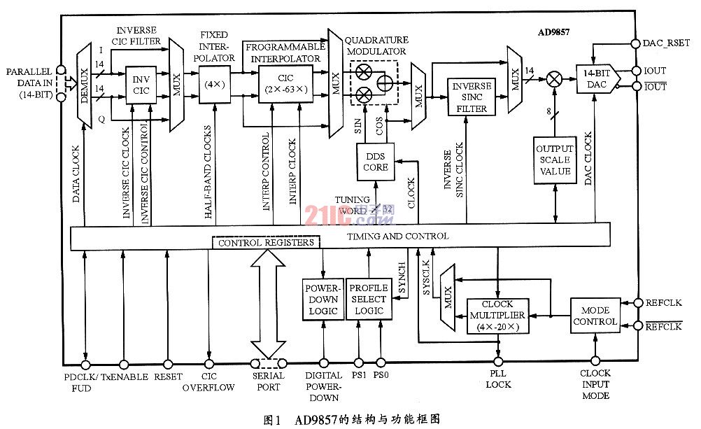
AD9857 has three working modes: quadrature modulation mode, single frequency mode and interpolated digital-to-analog conversion mode. Choose quadrature modulation mode here. The core part of AD9857 is the interpolation filter and quadrature digital mixer. The interpolation filter increases the sampling rate of the output signal by adding a new sample value—zero value near the original sample value, but when a zero value is inserted into the data in the time domain, the signal will produce the original signal spectrum in the frequency domain Mirror. Therefore, the image spectrum needs to be filtered through a low-pass filter. The orthogonal digital mixer digitally mixes the interpolated I / Q signal with the orthogonal carrier signal to complete the up-conversion process. The quadrature carrier signal is generated by the direct digital frequency synthesizer DDS, and its carrier frequency can be controlled by a 32-bit register, with high frequency accuracy.
A serial communication cycle of AD9857 is divided into the following two stages:
The first stage is the instruction cycle, which is the writing of the instruction byte of the AD9857. The instruction byte provides information about the data transmission cycle to the serial port control of the AD9857, and can determine whether the upcoming data transmission is read or write, the number of bytes of data transmission, and the register address of the first byte transmitted.
The second stage is the data transmission cycle. The first 8 SCLK rising edges of each communication cycle are used to write the instruction byte of the AD9857, and the remaining SCLK rising edges are for the second phase of the communication cycle, that is, data transmission between the AD9857 and the system controller. All data transmission of AD9857 is registered on the rising edge of SCLK and sent out on the falling edge. Figure 2 shows the timing diagram of register data write.
The SYNCIO signal can be used for serial port synchronization. After a period of transmission, in order to prevent the loss of symbol synchronization, the SYNCIO signal should be pulled to a high level for a clock cycle, and then pulled low again, that is, the next communication cycle begins. 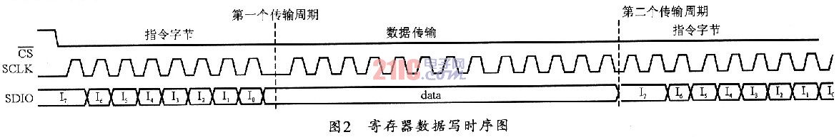 In this system, AD9857 is configured as orthogonal working mode. There are 8 register groups to be set, with addresses from 00h to 07h. The other 18 registers have nothing to do with this working mode, so no setting is needed. A communication cycle in the serial port can only transfer up to 4 bytes of data, so the register group should be written in two communication cycles. In two communication cycles, the first instruction byte and four bytes of register data constitute the first communication cycle; the second instruction byte and the other four bytes of register data constitute the second communication cycle.
The address range of the internal control register is 00h to 19h, of which 00h and 01h are shared. Set the operation mode such as phase loop failure processing. It is divided into 4 groups of registers with the same structure from 02h to 19h, each group is 6 byt-e in length, which contains the frequency control word of DDS, the interpolation multiple N of the CIC programmable interpolation filter and the output gain control. The value of each group can be set in advance. When the AD9857 is working, the desired function group can be selected by directly configuring the pins PS0 and PSl to achieve the purpose of quickly changing the working parameters.
The calculation formulas needed in this process are: 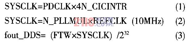
The reference clock input of this system is a single-ended clock of 10 MHz, and the PLL clock multiple is set to PLL_MUL = 4, then the system clock is SYSCLK = 40 MHz. The system requires a parallel port data input rate of PDCLK = 1.25 MHz, according to the formula: 
The interpolation multiple of the CIC filter is N_CIC = 8, the carrier frequency of the AD9857 is 4 MHz, the output frequency of the mixer DDS is fout_DDS = 4 MHz, and its frequency control word register FTW is set to 0x19999999. 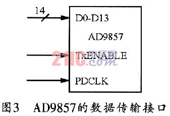
The functions of each pin are:
DO-D13: data transmission port, 14-bit parallel port;
PDCLK: input data synchronization clock, 2.5 MHz, provided to FPGA by AD9857;
TxENABLE: transmission enable signal, when the signal is 0, the input data is masked, and 0 is automatically filled in the I / Q channel; when the signal is 1, the data is received, and when the first rising edge comes, it starts to receive data.
The data is transmitted to the AD9857 through the 14-bit parallel data interface, and the I / Q channel data is transmitted alternately. Every two data transmission matches a set of legal I and Q sampling data. The two channels of data then pass through the inverted CIC interpolation filter to pre-compensate the attenuation caused by the CIC filter. After that, the data flows through a fixed interpolation filter with a interpolation factor of 4 and a programmable CIC filter. Among them, the interpolation rate of the CIC filter can be set through a register, usually set to 4 times the interpolation, and the signal sampling rate can be improved by the two-stage interpolation filter, and the low-pass filter filters out the image frequency generated by the interpolation. Finally, the signal enters the quadrature modulator and performs digital mixing (DDS) with the quadrature carrier signal to complete the up-conversion process. The up-converted signal undergoes D / A conversion to generate an analog intermediate frequency signal output. The output analog signal is output through the differential signal IOUT, and its output current range is 0 to 20 mA.
In this design, the AD9857 external crystal oscillator uses 10 MHz, and the internal frequency is multiplied by 4 times, and the working clock is 40 MHz. The internal programmable CIC interpolation system is 8, and the direct digital frequency synthesizer DDS generates a 4 MHz carrier signal. The AD9857 receives two IQ signals from the FPGA. After being interpolated by 32, it performs quadrature modulation with a 4MHz carrier. Afterwards, it is converted into a current signal after D \ A conversion, and finally the current signal is converted into Voltage signal. Because there is mirror frequency interference in the output signal of AD9857. Analog band-pass filters can be used for signal processing. The pass-band frequency of the band-pass filter is 3 MHz-5 MHz, and the pass-band attenuation is very small. Finally, the signal is differentially amplified by the AD8139 and sent to the power line coupling module.
can be divided into wrought copper and copper alloy solder joint
pressure fittings by different functions.Standard: EN1254-1, ANSI B16.22 The structure and dimension of each fitting is customizable, ensuring customers are getting the right fitting for their needs.Our parts have been exported to over 50 countries all over the world.
The article introduces the working principle and use method of AD9857, and discusses the configuration of AD9857 and the design method of related circuits in detail for the design of power line communication transmitter.