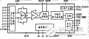
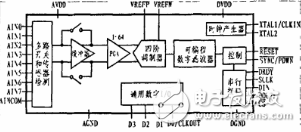
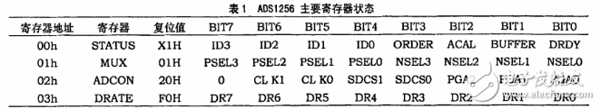
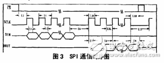
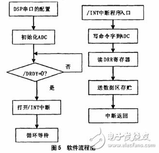
The geological detection system utilizes a 32-bit floating-point TMS320C6713 as the central controller. Leveraging its highly optimized architecture and unique command set, the ADS1256 efficiently collects data, enabling real-time control, analysis, and processing of signals. This combination ensures high precision and reliability in complex geological applications. The internal structure of the ADS1256 is illustrated below. The device comprises an analog multiplexer (MUX), input buffer (BUF), programmable gain amplifier (PGA), fourth-order Δ-Σ modulator, programmable digital filter, clock generator, controller, and a serial SPI interface. It is designed for low-frequency applications, supporting up to 30,000 samples per second (SPS). The chip features a comprehensive self-calibration and system correction mechanism, along with powerful computing capabilities—2400MIPS and 1800MFLOPS—with two on-chip multipliers. These features make it ideal for multi-channel AD acquisition systems, where the TMS320C6713 provides the necessary real-time signal processing power. Additionally, the TMS320C6713 has two independent MCBSP ports, which can be configured to manage the SPI interface and communicate with the ADS1256 effectively. ADS1256 Internal Structure Diagram To enhance performance, multiple ADS1256 units are used in parallel within the system. All ADCs share the same system clock, ensuring synchronized sampling across all channels. To simplify hardware design, only one interrupt pin is used in the system. Below is a schematic showing the connection between the DSP and one of the ADCs. The ADS1256 communicates with the DSP’s Multichannel Buffered Serial Port (MCBSP) via the SPI interface, allowing efficient data transfer and control. System Schematic The ADS1256’s functionality is primarily controlled through 11 internal registers that configure various operational parameters such as sampling rate, analog multiplexer settings, PGA configuration, I/O selection, and self-calibration. Table 1 summarizes the main register states, including the status register (s, rAll7S), MUX register, ADCON register, and DRATE register, which are essential for controlling the ADC at a 300MHz clock frequency. Table 1: Main Register Status of ADS1256 The ADS1256 uses a four-wire SPI communication interface consisting of SCLK, DIN, DOUT, and /CS. It operates in slave mode, and the DSP controls the internal registers through the SPI bus. During communication, the /CS line must remain low. The DRDY pin indicates when a conversion is complete, and it goes low once data is ready for reading. Data is transferred synchronously using the SCLK signal, with data being written on the falling edge and read on the rising edge. Maintaining a clean SCLK signal is critical to avoid data errors. Figure 3 illustrates the SPI timing relationship. The TMS320C6713 features two Multi-Channel Buffered Serial Ports (MCBSP), which support SPI protocol and multiple communication modes. When configured in clock stop mode, the MCBSP is compatible with SPI. The MCBSP supports two SPI transmission formats, which can be selected using the CLKSTP bit in the SPCR register. The ADS1256 connects to the DSP via its SPI interface, operating in slave mode with the SCLK generated by the DSP. The /CS signal enables communication, while the /DRDY signal indicates when data is ready. This signal is typically connected to a DSP interrupt to trigger data retrieval. Notably, the /DRDY signal remains high during parameter changes or calibration and returns to low once valid data is available. Commands from the DSP are sent through the DIN pin, and internal registers control the ADC's operation. The software configuration involves setting up the TMS320C6713’s serial port and defining the communication protocol with the ADS1256. The serial communication word module is shown in Figure 5. The DSP generates a 1MHz serial clock, with each communication word consisting of 32 bits: 8 bits for the instruction and 24 bits for the data. The FSXO frame sync signal is active low and is generated before each serial word. Both the FSXO and data are transmitted on the falling edge of CLKR0, ensuring the ADS1256 samples data on the rising edge. This setup guarantees accurate and reliable data exchange between the DSP and the ADC. A fishing rod Braided Sleeve is a protective covering made of braided material that is designed to be slipped over a fishing rod. It provides added protection to the rod, preventing it from getting scratched or damaged during transport or storage. Fishing Rod Braided Sleeve,Fishing Rod Sleeving,Pet Fishing Sleeving,Fishing Rod Sleevings Dongguan Liansi Electronics Co.,Ltd , https://www.liansisleeve.com