Zgar International (M) SDN BHD , https://www.zgarvape.com
Speaking of touch delay switches, I'm sure many people find them quite intriguing. They're commonly seen in hallway lighting systems, where some operate with a touch mechanism while others respond to voice commands. Today, I want to focus on touch delay switches and explain their wiring. Below is a detailed guide on how to wire a touch delay switch.
**Understanding the Touch Delay Switch**
Delay switches come in various types, including touch delay and sound-controlled versions. By simply touching the switch's pad or making a sound, these switches can automatically activate lights. Once activated, they will remain on for 30 to 75 seconds before turning off automatically. This energy-efficient design is often recommended by energy ministries. The touch delay switch operates based on the same principle as a tester pen, using a high-value resistor to create a low-voltage current through the human body. This current eventually flows to the ground, triggering a circuit that starts the timer and powers the light.
**How Does the Touch Delay Switch Work?**
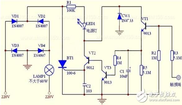
In the switch circuit, an electret microphone MIC is used for acoustic detection, and a transistor T2 acts as an amplifier. When there’s no sound, T2 remains in a saturated conducting state. However, when a sound is detected, the microphone picks up the signal, turning off T2. For brightness detection, a photoresistor RG is used. The circuit employs a CMOS digital integrated circuit CD4011, containing four 2-input NAND gates. One of these gates serves as a direct discriminator circuit, while the other three are connected as inverters for amplification purposes. Components D6, R6, and C4 form a delay circuit. The switch uses a thyristor T1. Diodes D1 to D4 and thyristor T1 form a controllable rectifier circuit. When T1 is activated, the bulb lights up; when deactivated, the bulb turns off.
**Step-by-Step Guide to Wiring a Touch Delay Switch**
The touch delay switch features a metal sensing chip on its exterior. A human touch generates a signal that triggers a transistor to conduct, charging a capacitor. This capacitor maintains a voltage to keep the FET conducting, thereby lighting the bulb. Once the touch is removed, the capacitor stops charging. After a set period, the capacitor discharges, lowering the FET's gate voltage and cutting off the circuit, thus turning off the bulb.
The touch delay switch circuit is divided into two parts: the ordinary lighting circuit on the right side of the dotted line and the electronic switch portion on the left. VD1 to VD4 and VS form the main switch circuit, while IC constitutes the switch control circuit. Under normal conditions, VS remains off, and the light stays off. VD1 to VD4 provide a 220V pulsating DC current via R5 current limiting, VD5 voltage regulation, and C2 filtering, delivering approximately 12V DC power to IC. At this point, the LED lights up, marking the switch's location for easy nighttime access.
IC is a dual-D flip-flop, and only one of the D flip-flops is used, connected to a monostable circuit. In a steady state, pin 1 outputs a low level, keeping VS off. When the hand touches the electrode M, the human body leakage current divides between R1 and R2, turning the monostable circuit on during the positive half-cycle. Pin 1 then outputs a high level, applying R4 to the VS gate, turning VS on and lighting the bulb. During this time, pin 1 outputs a high level, and capacitor C1 charges through R3, gradually increasing the level at pin 4 until the transient ends, returning the circuit to a steady state. Pin 1 abruptly changes to a low level, removing the trigger voltage from VS. The alternating current crosses zero, turning off the light.
**A Closer Look at the Touch Delay Switch Circuit**
The figure illustrates the experimental circuit for the touch delay switch. It includes a full-wave bridge rectifier circuit made of rectifier diodes VD1 to VD4, serving as an integrated circuit power supply, and a four-input NAND gate 4011 along with a unidirectional thyristor VS1 forming the touch switch circuit. The full-wave bridge rectifier circuit provides up to 200V pulsating DC power, which is divided by resistors R1 and R2 and filtered by capacitor C1 to produce around 13V DC power for IC operation. During the illumination of lamp EL, the total current of the 4011 under steady-state operation is less than 20μA, and the current when the lamp is off is nearly immeasurable, showcasing the low power consumption of the CMOS integrated circuit. Moreover, when the illumination lamp EL is lit, the partial voltage drop across R2 is 2V, allowing the 4011 to continue functioning, highlighting the advantages of the CMOS digital integrated circuit.
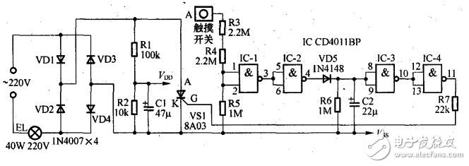
When the metal piece A end is touched by hand, the inductive alternating current signal is applied to the input terminal of IC-1 through the step-down resistors R3 and R4. During the positive half-cycle, pins 1 and 2 of IC-1 are at a high level, causing the output terminal to drop to a low level, and the IC-2 output terminal 4 to rise to a high level. The timing capacitor C2 is charged through the switching diode VD5, raising the IC-3 input terminal to a high level, and its output terminal 10 pin to a low level. The IC-4 output terminal 11 is high, and is applied to the unidirectional thyristor control electrode G through resistor R7, triggering VS1 to turn on and illuminating the load lamp EL. As C2 gradually discharges through the timing resistor R6, causing the voltage to drop below the CMOS gate turn-on voltage, the IC-3 output rises to a high level, the IC-4 output falls, the unidirectional thyristor blocks, and EL goes out. With R6 at 1MΩ and C2 at 10μF, the touch switch control delay is about 17 seconds; when C2 is changed to 22μF, the delay doubles; with C2 at 47μF, the delay is sufficient.
In the touch switch circuit, R5 is a pull-down resistor. Although its resistance value is 1MΩ, the input voltage of the NAND gate IC-1 is low, indicating the high input impedance of the CMOS digital integrated circuit. The remaining input terminals of the four-input NAND gate 4011 cannot be left floating and are instead connected in parallel as non-doors. The IC can also use four 2-input or non-gate 4001.
**Conclusion**
As we navigate life, we encounter numerous devices whose proper usage might be unclear. Through this explanation, I hope you now have a clearer understanding of touch delay switches and their wiring. Should you ever need to install one in the future, these instructions should make the process straightforward and ensure excellent results.