![]()
Probe for domestic switch needle KG-300K needle head diameter is 3.0mm, typically an open switch needle.
![]()
Crystal oscillator.
![]()
Quartz Oscillator 3225 20M OSC.
The CD4093 consists of four 2-input Schmitt trigger circuits. Each circuit is a 2-input NAND gate with Schmitt trigger functionality on both inputs. These gates open and close at different points on the rising and falling edges of the signal. The difference between the rising voltage (VP)T and the falling voltage (VN) is defined as the hysteresis voltage (â–³VT).
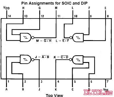
CD4093 Pin Diagram
CD4093 Pin Functions:
E - Data input terminal, J - Data output terminal, B - Data input terminal, F - Data input terminal, K - Data output terminal, C - Data input terminal, G - Data input terminal, L - Data output terminal, D - Data input terminal, H - Data input terminal, M - Data output terminal, VDD - Positive Power, VSS - Ground.
Absolute Maximum Ratings:
DC Supply Voltage (VDD) -0.5 to +18 V
DC Input Voltage (VIN) -0.5 to VDD +0.5 V
Storage Temperature Range (TS) -65°C to +150°C
Power Dissipation (PD) Dual-In-Line Normal Double Row Package: 700 mW
Small Outline Package: 500 mW
Lead Temperature Soldering Temperature (TL) Soldering, 10 seconds): 260°C
Recommended Operating Conditions:
DC Supply Voltage (VDD) 3 to 15 V
DC Input Voltage (VIN) 0 to VDD V
Operating Temperature Range (TA) -40°C to +85°C
DC Electrical Characteristics:
Symbol
Parameter
Conditions -40°C +25°C +85°C
Units
Typically Min Max Min Max Min Max
IDD Quiescent Device Current VDD = 5V 1.0 1.0 7.5 μA VDD = 10V 2.0 2.0 15.0 VDD = 15V 4.0 4.0 30.0
VOL LOW Level Output Voltage Output Low Voltage VIN = VDD, | IO | < 1μA VDD = 5V 0.05 0 0.05 0.05 V VDD = 10V 0.05 0 0.05 0.05 VDD = 15V 0.05 0 0.05 0.05
VOH HIGH Level Output Voltage Output High Level Voltage VIN = VSS, |IO| < 1μA VDD = 5V 4.95 4.95 5 4.95 V VDD = 10V 9.95 9.95 10 9.95 VDD = 15V 14.95 14.95 15 14.95
VT- Negative-Going Threshold Voltage (Any Input) Negative Threshold Voltage (Any Input) |IO| < 1μA VDD=5V, VO =4.5V 1.3 2.25 1.5 1.8 2.25 1.5 2.3 V VDD=10V, VO = 9V 2.85 4.5 3.0 4.1 4.5 3.0 4.65 VDD=15V, VO=13.5V 4.35 6.75 4.5 6.3 6.75 4.5 6.9
VT+ Positive-Going Threshold Voltage (Any Input) Forward Threshold Voltage (Any Input) | IO| < 1μA VDD = 5V, VO = 0.5V 2.75 3.6 2.75 3.3 3.5 2.65 3.5 V VDD = 10V, VO = 1V 5.5 7.15 5.5 6.2 7.0 5.35 7.0 VDD = 15V, VO = 1.5V 8.25 10.65 8.25 9.0 10.5 8.1 10.5
VH Hysteresis (VT+ - VT-) (Any Input) Hysteresis (VT+ - VT-) (Any Input) VDD = 5V 0.5 2.35 0.5 1.5 2.0 0.35 2.0 V VDD = 10V 1.0 4.3 1.0 2.2 4.0 0.70 4.0 VDD = 15V 1.5 6.3 1.5 2.7 6.0 1.20 6.0
IOL LOW Level Output Current Output Low Current (Note 3) VIN = VDD VDD=5V, VO =0.4V 0.52 0.44 0.88 0.36 mA VDD=10V, VO=0.5V 1.3 1.1 2.25 0.9 VDD=15V, VO =1.5V 3.6 3.0 8.8 2.4
IOH HIGH Level Output Current Output High Level Current (Note 3) VIN = VSS VDD=5V, VO =4.6V -0.52 0.44 -0.88 -0.36 mA VDD =10V, VO=9.5V -1.3 -1.1 -2.25 -0.9 VDD=15V, VO=13.5V -3.6 -3.0 -8.8 -2.4
IIN Input Current Input Current VDD=15V, VIN = 0V -0.3 -10-5 -0.3 -1.0 μA VDD=15V, VIN =15V 0.3 10-5 0.3 1.0
AC Electrical Characteristics:
Symbol
Parameter
Conditions
Minimum Typical Maximum
Units
tPHL, tPLH Propagation Delay Time Transfer Delay Time VDD = 5V 300 450 ns VDD = 10V 120 210 VDD = 15V 80 160
tTHL, tTLH Transition Time Transition Time VDD = 5V 90 145 ns VDD = 10V 50 75 VDD = 15V 40 60
CIN Input Capacitance Input Input (Any Input) 5.0 7.5 pF
CPD Power Dissipation Power Capacitance (Per Gate) 24 pF
Typical Application Circuit:
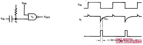
Negative Edge Trigger
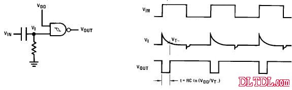
Positive Edge Trigger
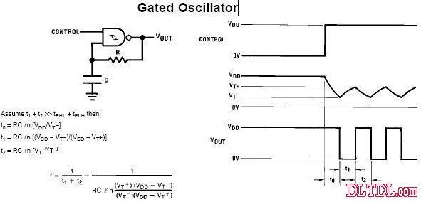
Controlled Oscillator
Application Circuit: Touch Switch
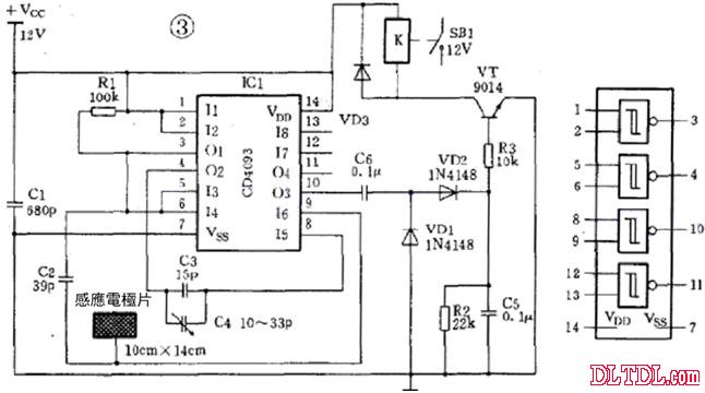
This circuit is primarily composed of a four-two input NAND gate integrated circuit CD4093. A NAND gate (1, 2, 3, IC1) of R1, C1 and CD4093 forms a 400Hz square wave oscillator. The square wave of the oscillator output is divided into two paths: one path is directly sent to a NAND circuit (4, 5, 6 feet, IC2); the other path is sent to a NAND gate (8, 9, 10, IC3) via a capacitor C2. Since IC2 is connected in the form of a NOT gate, its input and output potentials are 180° out of phase, and the signal output from IC2 is coupled to the other input of IC3 via C3 and C4. Since the levels of the two inputs of IC3 are the same but the phases are opposite, as long as IC1 oscillates normally, at least one of the two inputs of IC3 is at a low level, so the output of IC3 is a stable high level. Due to the action of C6, VT1 is turned off. However, if the input signal of any input of IC3 is canceled or the amplitude of the signal is lowered below the input start level of the gate, IC3 outputs a square wave signal. When a conductor approaches the sensing electrode, part of the signal coupled by C2 to the input pin 9 of IC3 is shunted to ground. If the amplitude of the signal after shunting is lower than the threshold level of the NAND gate, IC3 outputs a square wave signal. After the signal is rectified by VD1 and VD2, the switching tube VT1 is turned on, and the power of the relay is turned on to make it close. Capacitor C4 is the sensitivity adjustment capacitor. If the circuit needs to work with maximum sensitivity, you can adjust C4 to make the relay just pick up, then adjust C4 to make the relay just disconnect, then seal C4 with high frequency wax or insulating paint.
Mobile Computer,Android Pda With Keyboard,Pos Terminal Temperature,Barcode Scanne Pda