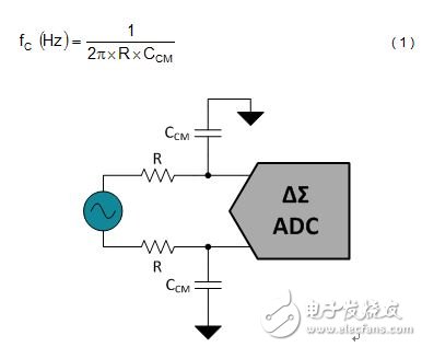
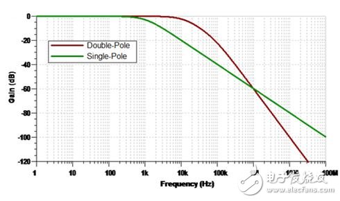
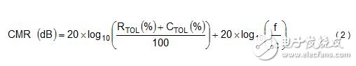
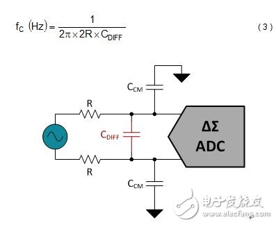
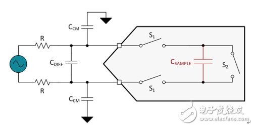
The anti-aliasing filter design includes an oversampling architecture and a complementary digital decimation filter. This oversampling architecture places the Nyquist frequency away from the signal bandwidth, while the digital decimation filter attenuates most of the unwanted out-of-band signals. When combined, they can achieve a more free anti-aliasing filter response, which can be achieved with just a few discrete components. Figure 1: Blocking these aliases with a suitable anti-aliasing filter We know that using anti-aliasing filters in high-precision ADC applications is beneficial, but designing an appropriate anti-aliasing filter is equally important—if you are not careful, just like removing harmful errors from the system, It is easy to introduce harmful errors into your system. When designing anti-aliasing filters for your application, consider the following three general guidelines: 1. Choose your filter cutoff frequency The simplest anti-aliasing filter is a single-pole, low-pass filter, as shown in Figure 2, which uses a series resistor (R) and a common mode capacitor (CCM). The first step in designing this filter is to select the desired cutoff frequency, fC. At fC, the filter's response rolls down to -3dB and continues to decrease at -20dB/decade over the frequency domain. Select a cutoff frequency that is at least ten times lower than the ADC modulator sampling frequency, fMOD, with the goal of suppressing out-of-band noise by a factor of 10 or more at these frequencies. For increased attenuation, the cutoff frequency is further reduced by increasing the values ​​of R and CCM. As I mentioned in the previous article, the purpose of your digital decimation filter is to help, so there is no need to set your anti-aliasing filter cutoff frequency immediately after the desired signal bandwidth. Equation 1 calculates the cutoff frequency of the single-pole, low-pass filter to be -3dB: Figure 2. Unipolar, low-pass filter on the ADC input Sometimes a single-pole, low-pass filter may not be enough. Applications such as vibration sensing may use less oversampling to analyze signals over a wider bandwidth. This brings the passband of the digital decimation filter closer to fMOD and makes the roll-off space of the anti-aliasing filter smaller. In these cases, you can add a second or third pole with an extra RC pair to achieve a more sensitive filter response. Shown in Figure 3 is the response of the unipolar and bipolar filters designed for the ADC; this ADC samples the input at fMOD = 1MHz. The flat passband of the bipolar filter scales out to approximately 20 kHz and is still capable of achieving -60 dB attenuation at 1 MHz. Figure 3. Frequency response of unipolar and bipolar low-pass filters 2. Consider the relationship between differential and common mode filters Many ADCs convert the voltage between two independent inputs (such as INP and INN), so designers often put a common-mode filter on each input to maintain system common-mode rejection (CMR). However, component tolerances will cause any two filters to mismatch and will reduce CMR performance over the frequency range because the filtering operations on the common signal are different. This produces a differential signal error through the common mode to differential conversion known. Equation 2 uses the resistor tolerance, RTOL, and capacitor tolerance, CTOL, to calculate the CMR of the common mode anti-aliasing filter at the specified frequency: For applications that require high CMR, as shown in Figure 4, consider adding a differential filter to complement the two common mode filters. By increasing the differential capacitor CDIFF to 10 times larger than the CCM, the differential cutoff frequency is set to be 10 times lower than the common mode cutoff frequency. This mitigates the errors introduced by common mode component mismatch and produces a more sensitive overall filter response. Equation 3 calculates the cutoff frequency of the differential low pass filter. It should be noted that there is an additional factor of 2 in the denominator. Figure 4. Common mode filter with a differential filter added 3. Select the appropriate component value Adding resistors to the signal path introduces unwanted noise and errors into the measurement, so it is necessary to keep them within reasonable limits whenever necessary. Resistor noise—also known as Johnson or thermal noise—can be modeled as a voltage source in series with your ideal “noise-free†resistor. In general, you don't want resistor thermal noise to occupy the entire signal chain, so it's important to keep it below the noise floor of the ADC. Equation 4 calculates the noise density of the resistor thermal noise, vn: Here, k = Boltzmann constant (1.38E-23 J/K), and T is the temperature value in Kelvin. The series resistor also introduces a small offset voltage when the input bias current occurs. Although you may be able to calibrate this value later, it is still necessary to limit the size of the resistor as much as possible, especially if the bias current is likely to become very large. Unlike filter resistors, the higher the value of the capacitor you can use, the better the effect. To understand why, you must know how the ADC samples the input. The delta-accumulated ADC input without the integrated buffer is directly connected to the switched capacitor sampling structure of the ADC modulator. This sampling structure consists of a switching network and a sampling capacitor with a capacitance of approximately 10 pF or 20 pF. Figure 5 shows a simplified example. Figure 5. Simplified switched capacitor sampling structure in an ADC During the sampling period, this switched capacitor circuit places a transient load on the external circuit. This filter capacitor helps reduce the sample charge injection from the modulator and provides some of the instantaneous current required for charging the sampling capacitor, CSAMPLE. The larger the filter capacitor, the more charge is available. Due to its high Q factor, low temperature coefficient, and stable electrical characteristics, use ceramic capacitors of type NP0/C0G. Larger capacitor values ​​also improve AC specifications such as total harmonic distortion (THD), but it is important to keep in mind that this increases the filter's RC time constant and requires a longer settling time. I hope these three guidelines have prepared you for the next anti-aliasing filter design. Sand Casting is made of clay-bonded sand as a molding material. It is a process method with a long history. It is also the most widely used process method. In the development of various chemical bonding sand, the clay wet sand is still the most important molding material, and its application range is wide and the consumption is large, and it is not comparable to any other molding material. It is reported that in the steel castings of the United States, more than 80% of the clay-wet molding sand is used; in Japanese steel castings, more than 73% of the clay-wet molding sand is used. Sand Casting,Sand Casting Tube,Sand Casting Process,Inron Sand Casting Pats Dongguan Formal Precision Metal Parts Co,. Ltd , https://www.formalmetal.com