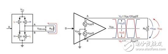
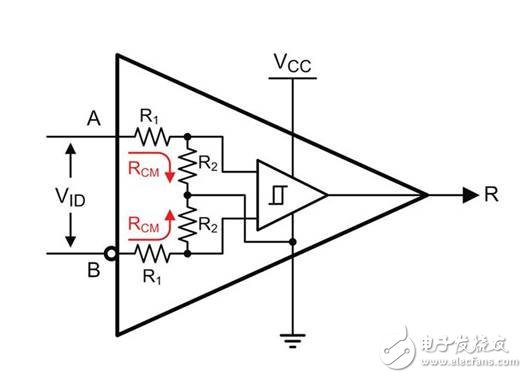
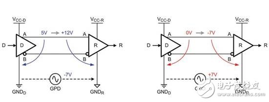
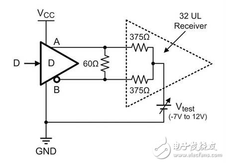
With its robustness and high reliability, RS-485 has become the most commonly used application interface technology in noisy industrial environments worldwide. The combination of a wider operating range and higher rejection performance has resulted in transceiver designs that have surpassed the original RS-485 standard (EIA/TIA485). The new transceiver specifications give these performance improvements in the component datasheets, however, these specifications are often misinterpreted by end users, system designers. For example, confusion is often seen when comparing the maximum voltage levels of the given transceivers under the Absolute Maximum Ratings (AMR) section and the Recommended Operating Conditions (ROC). Can the transceiver reliably transmit data at absolute maximum ratings? Why is the input voltage under ROC much smaller than the value in AMR? How is the common mode voltage range defined? Since the transceiver data sheet rarely provides a detailed explanation of these parameters, this article will adjust this. We first explain the basic workings of the transceiver, and then how to derive the common mode voltage term from it. Finally, we will explain the maximum working conditions. driver The driver portion of the transceiver consists of an H-bridge output stage. A logic high on data input D turns on transistors Q2 and Q3. This will drive current from the A terminal to the B terminal. The logic low on D turns on Q1 and Q4 and drives the current in the opposite direction, from B to A. The internal resistance of the reverse leakage protection diode and the transistor on-resistance form a voltage divider with an external differential load resistor RD. This makes the line voltages VA and VB significantly smaller than the supply voltage VCC (Fig. 1). The complementary line voltages thus obtained, VA and VB, represent two DC voltage levels that oscillate around the average DC level (which is the common voltage of the two bus lines). This voltage is called the driver common mode output, or the output offset voltage, VOS. This common mode voltage is obvious, and the differential output voltage is the amount of line voltage generated by making the two equations equal. Therefore, the driver can be represented as a signal source having a common mode component VOS. The common mode component VOS is overlapped by complementary differential components. figure 1 receiver The receiver portion of a transceiver includes a resistor divider on each input, R1/R2, followed by a comparator. The voltage divider attenuates the input signal, VA and VB, at a 10:1 ratio. This ratio determines the maximum applicable receiver input voltage on A and B. Since the voltage divider is referenced to the receiver ground, the common mode and differential voltage components have the same attenuation rate. The differential comparator then removes the common-mode signal and reacts only to the differential input signal, VID = VA - VB. Therefore, the standard RS-485 transceiver outputs R, which goes high when VID is greater than 200mV and goes low when VID is less than 200mV. Figure 2 shows the common-mode input resistance with RCM = R1 + R2 for each receiver input and the differential input resistance for RIN = 2 RCM. RCM results in a common-mode load for each bus line, that is, the common-mode voltage drive current on both lines flows through the RCM to the receiver ground. In contrast, RIN causes differential load current to flow between bus lines. figure 2 Maximum receiver input voltage range The RS-485 standard specifies a common-mode input range of -7V to +12V and a maximum ground potential difference (GPD) of ±7V between the driver and the remote receiver. Figure 3 shows an example of a data link for the maximum possible bus voltage. In this case, the link is an unterminated point-to-point connection. A single receiver represents a light load, causing the line voltage to swing throughout the power rail. image 3 An extreme case is when the output of the driver is 5V relative to the driver ground (GNDD), at which point GPD = -7V. In this case, the maximum positive receiver input voltage relative to the receiver ground (GNDR) is +12V. The other extreme case is that the driver output voltage is 0V with respect to GNDD, at which point GPD = +7V. In this case, the maximum negative receiver input relative to GNDR is -7V. To ensure reliable data transfer, the maximum receiver input voltage range is between +12V and -7V. It should be noted that the GPD is the potential difference between the driver and the receiver ground and represents the second common mode voltage added to the driver output offset. The overall common-mode voltage of a data link, VCM, is VCM = VOS + GPD. A further requirement for RS-485 is that the driver must be able to drive 32 unit loads on a full GPD of ±7V. One unit load represents a common mode load and is defined as a 1 mA DC input current at a 12V DC input voltage. This will produce a 12kΩ DC input resistance. Traditional transceivers typically have a 1UL common-mode load, while modern components typically have a unit load of 1/8 UL, which means that the input current is 1/8 of the conventional input current, or 8 times higher than the input resistance to ground. To test the maximum common mode load, the test circuit in Figure 4 is typically used. Figure 4 Here, a 60Ω differential resistor represents two 120Ω termination resistors at each end of the bus. The 375Ω resistor is similar to 32 unit loads and can be a 32 x 1UL transceiver or a 258 x 1/8UL transceiver. The ±7V symmetrical GPD is replaced by a test voltage ranging from -7V to +12V for the purpose of testing symmetric transceiver input performance. For example, if the drive is capable of providing a full supply range on its input, the output is 5V and VTEST = -7V, the input voltage of the receiver relative to the receiver ground will be +12V. For a 0V output voltage and VTEST = +12V, the input voltage of the receiver relative to the receiver ground will be -12V. The minimum and maximum transceiver input voltage ratings are -12V and +12V, respectively. Since reliable data transmission must be ensured within this voltage range, these values ​​are rated for the recommended operating conditions (ROC). It should be noted that these recommended maximum values ​​assume a maximum driver output range of 0V to 5V. The actual common mode voltage range is much smaller. For a 5V transceiver, VCM+ is calculated as VCM = 2.5V + 7V = +9.5V, while VCM- = 2.5 – 12V = -9.5V. Absolute maximum rating In applications where the RS-485 data line is parallel to the 24Vdc power line, safety must be implemented in the transceiver design to avoid damage to the device in the event of a short-circuit fault such as damage to the cable insulation of the power and data lines. . A common solution is to use high voltage transistors in the driver output stage. This output stage can adequately suppress short-time high-voltage transients and long-term over-voltage. A common requirement in industrial systems is that the transceiver must be able to withstand permanent shorting of the 24V power cord. However, external transient voltage suppressors (TVS) that protect the transceiver from 24V damage are not available. Conversely, any 24V component used must first protect the 24V supply. In fact 24V is only a nominal value, and many power systems can exhibit a range of up to 35V. This increases the required TVS breakdown voltage to 36V. TVS diodes with such high breakdown voltages typically provide clamping voltages of up to 60V. In order to withstand these high transient voltages, the transceiver must provide a rejection voltage of 65V to 70V or more. These suppression voltage levels are those specified at the absolute maximum rating. Any higher voltage level will trigger the transceiver's internal electrostatic discharge (ESD) protection circuit. However, these ESD circuits are only designed for very short transient overvoltages and do not protect the device from long-term electrical overstress. The most important point is that never exceed the voltage level specified in the absolute maximum rating. Round Series Sensor Automatic Dustbin Stainless Steel Garbage Can,Round Series Sensor Automatic Dustbin,Round Series Sensor Dustbin,Round Series Automatical Indoor Dustbin NINGBO ZIXING ELECTRONIC CO.,LTD. , https://www.zixingautobin.com