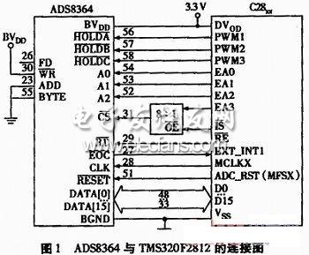
In practical engineering applications, it is often necessary to perform condition monitoring and fault diagnosis on various devices. First, the signals of each sensor are collected. In order to reduce the computing load of the host computer, a smart node based on DSP is designed. Realize functions such as signal acquisition and FFT transformation. 1 hardware design The hardware of the intelligent node mainly includes DSP processor, analog-to-digital converter, extended static memory, level conversion chip, CAN interface drive, optocoupler input and sensor conditioning and power supply circuit. The DSP processor uses TI's 32-bit fixed-point high-speed DSP chip TMS320F2812. The TMS320F28X series is the most advanced 32-bit fixed-point DSP chip in the world. Not only does it run fast, it has powerful processing power, and it has a rich set of on-chip peripherals for easy interface and modular design. It not only has digital signal processing capability, but also has powerful event management capability and embedded control function. It is especially suitable for measurement and control occasions with large-scale data processing, such as industrial automation control, intelligent instrumentation and motor servo control system. It adopts 8-level instruction pipeline, single-cycle 32 & TImes; 32-bit MAC function, and can execute 150 million instructions (150 MIPS) per second at maximum speed, ensuring the fast and real-time control and signal processing. In addition, MS320F2812 also integrates a wealth of external resources, including 16 12-bit ADC, 16 PWM outputs, 3 32-bit general-purpose timers, 128k 16-bit FLASH memory, 18kRAM memory, and peripheral interrupt expansion module (PIE) support. 45 peripheral interrupts with interfaces such as McBSP, SPI, SCI and extended CAN bus. The TMS320F2812 also supports up to 1M of external memory expansion. TMS32 0F2812 supports C/C++ programming language, its C language optimizer C compiler efficiency up to 90%, as well as virtual floating-point math function library support, can greatly shorten the development cycle of mathematical operations and control programs. The analog-to-digital converter uses TI's ADS8364, which is a 6-channel analog input, 16-bit parallel output analog-to-digital converter. The six analog inputs are divided into three groups (A, B, and C), each of which has a hold signal to achieve simultaneous sampling and conversion of all channels, making it ideal for multi-channel (multiple) acquisition systems. The ADS8364 provides a flexible high-speed parallel interface that can run in direct addressing, cyclic sampling, FIFO and other modes. The output data of each channel can be directly used as a 16-bit word, which can be directly connected to the digital signal processor TMS320F2812. Connected. Since data acquisition and FFT conversion require a large amount of data space, the TMS320F2812 has only 18 kbytes of RAM available on the chip, and it is distributed in five different areas, which cannot meet the requirements of use. Therefore, a 64 kbit 16-bit non-extension is extended externally. Wait for the static memory IS61LV6416. The key part of the intelligent node circuit design is the minimum system design of the TMS320F2812 chip and the interface design of the ADS8364. 1.1 Minimum system design of TMS320F2812 (1) Power supply and reset section: This design is powered by an external 5 V DC voltage. A 3.3 V core voltage VDD and a 1.8 V I/O voltage VDDIO voltage are generated by the DC/DC device. The power chip TPS767D318 is a dual-supply output, one for 3.3 V and one for 1.8 V. The maximum output current of each power supply is 1 A. The chip also provides two low-level reset pulses with a width of 200 ms. There are two kinds of reset signals in this design: power-on reset and manual reset. The power-on reset is generated by the chip TPS767D318, and the manual reset is generated by a circuit composed of resistors and capacitors. (2) Clock part: There are generally two ways to provide a clock for the DSP chip. One is the use of crystals and the other is the use of external active clock chips. This design uses the former. It utilizes the crystal oscillator circuit provided inside the DSP chip, and connects a crystal startable internal oscillator between x1 and x2 of the DSP chip. (3) Simulation part: This part will be used as the debugging and programming of the program. The 2812 chip provides five standard JTAG signals (TRST, TCK, TMS, TDI, TDO) and two emulation pins (EMU0, EMU1). 1.2 ADS8364 interface design The ADS8364 uses a +5V analog supply (AVDD) and a digital supply (DVDD), while its internal buffer uses the same +3.3 V voltage as the TMS320F2812. The buffer voltage (BVDD) allows direct connection to a 3 V or 5 V voltage system. The I/O voltage of the TMS320F2812 is +3.3 V, so if this component is used, the BVDD of the ADS8364 must be set to 3.3 V. In this design, the ADS8364 uses a 4 MHz clock. The throughput of each channel can be up to 200 ksps. Connect the address line A[2:0] of ADS to the address line of TMS320F2812. When A0 is connected to digital ground, A2 and A1 are connected to VCC to force ADS8364 into periodic mode. In this mode, the converter automatically samples six channels and transfers the data from A0 to C1 to the output. Byte mode can be enabled by connecting the BYTE pin of the ADS8364 to VCC. In this mode, to read data correctly from the ADC, two consecutive reads are required for each channel. The first reading is the high byte of the conversion data, and the second reading is the low byte. If the channel information is to be part of the data output, then the ADD pin of the ADS8364 should also be connected to VCC. When reading data, you need to read three times for each channel of the ADS8364. The channel and data information are read for the first time, and the high and low data are read twice. 1.3 ADC initialization operation Triggering the reset pin RST of the ADS8364 ensures that the read pointer points to the first data location. As part of the TMS320F2812 initialization, the general-purpose input and output port GPIOFO of the TMS320F2812 is supplied to the pin RST of the ADS8364. When the system clock is stable, it is triggered low, which ensures that the data output from the ADC corresponds to the arrangement of channels A0, A1, B0, B1, C0, C1. For each conversion channel, EOC is a low level signal. The ADS8364 provides three pulses to the TMS320F2812. Each pulse signal indicates the end of a transition. When the three pins of the ADC are simultaneously asserted low, the three channels are considered valid and converted simultaneously. Alternatively, the EOC pin can be tied to an interrupt pin on the TMS320F2812 to trigger a read cycle. The chip select CS of the ADS8364 is an active low level input signal. When CS is high, the parallel output pin is in a high-impedance state. When CS is low, the parallel data line reflects the current state of the output buffer. In order to properly read data from the ADS8364's parallel data bus, the ADS8364 must be selected by the Chip Select CS before it can be read. The read (RD) signal terminal of the ADS8364 is also an active low level signal. When CS is low, the contents of the registers in the ADS8364 will be updated on the falling edge of the read signal (RD). This means that the RD signal must be triggered before each read sequence in order to update the output buffer. The input data can be saved by setting the RD pin of the ADS8364 low by the interrupt subroutine of the TMS320F2812, and then setting the RD pin high. 2 software design In actual work, the intelligent node sends the collected data or spectrum value to the upper computer for storage and processing. The host computer communicates with the intelligent node through the CAN interface. The intelligent node program is developed in C language on the development tool Code Composer Studio provided by TI. In the development process, the C281×C/C++ header file library provided by TI was used. The header file library defines the registers of the F2812 in the form of structures and unions. The user can directly access the registers inside the processor through the C language. Since the MS320F2812 does not have independent program storage space and data storage space, it is uniformly addressed. Therefore, the user must first divide the storage space by configuring a link command file (.cmd file) as needed. In order to realize the FFT transformation of data, the FFT function library provided by TI company is also used in the development process. The FFT function library provides two modules of 32-bit complex FFT transform (CFFT32) and real FFT transform (RFFT32), which can perform complex and real FFT transforms of 128, 256, 512 and 1024 points. It should be noted that the data used in the transformation is in the Qx format, so the transformed result needs to be formatted to get the true value. The main program flow of the intelligent node is: after power-on, the program is initialized first, and after entering the main loop, data acquisition and threshold judgment are continuously performed. If the host computer command is received (CAN interface receiving interrupt), the program is transferred to the interrupt processing program, according to Different commands of the host computer select different processing methods. If the collected data exceeds the threshold, the alarm is sent to the upper computer. 3 Conclusion The intelligent node designed in this paper has been applied in many monitoring and fault diagnosis systems. It has been proved that the module works reliably and can meet the needs of distributed data collection and monitoring in engineering. Mirror Heating Elements can be used in many field. Such as car rearview mirror.bathroom mirror.camera even in flower showcase freezer.With the property of automatically power change,the PET heating film can convert the electrical energy into thermal energy efficiently which makes the mirror suface's temperature rise to prevent steam from condensing. Not only did we supply the good quality of manufactured goods but also offer service of custom-made mirror heating film.We look forward to build business cooperation with customers worldwide. Mirror Heating Elements Rearview Mirror Heating Film,Ptc Heating Film , Mirror Heating Elements,Bathroom Mirror Heating Film ShenZhen XingHongChang Electric CO., LTD. , https://www.xhc-heater.com