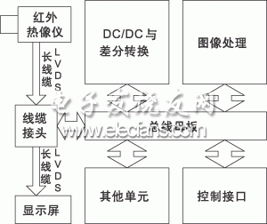
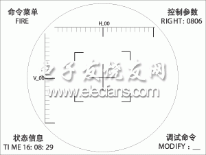
The electronic image-spinning system introduced in this paper uses Altera's StraTIxII series FPGA chip and ADI's ADSP2183 as the core to meet the system's requirements for functionality, real-time and accuracy. System principle and basic structure The block diagram of the TV viewing system is shown in Figure 1. The system consists of an infrared camera, a main image processing board, a DC/DC and differential conversion board, a bus motherboard, a control interface board, and a display screen. Figure 1 block diagram of the TV viewing system First, the infrared camera generates digital video image data of the viewing scene and transmits it to the system bus as an LVDS signal. The LVDS video signal is used here, mainly considering that the TV viewing system requires working in a very harsh physical environment, and the LVDS method has good anti-electromagnetic interference (EMI) capability, which can well ensure the video signal in a longer distance condition. The quality of the transmission. The derotation processing module comprises four functional units: (1) DC/DC conversion, LVDS and LVTTL mutual conversion unit; (2) system control interface unit; (3) image processing unit; and (4) other units. The functional unit (1) completes the system power supply and LVDS digital differential video to LVTTL digital video conversion; the system control unit (2) includes two serial interfaces and data exchange mailboxes to complete information exchange; the functional unit (3) is the core of the system In part, it implements image processing and guarantees accuracy; unit (4) is mainly the design and data storage unit of system electromagnetic compatibility. The image processing module completes the pipeline processing of the digital video signal. All the workflows use the FPGA device to realize the correction, rotation, accuracy calculation, real-time image interpolation, etc. of the field center under the control of the DSP. Finally, the number processed by the erasing rotation is processed. The video stream is then transmitted to the terminal display by the LVDS Driver portion of the DC/DC and differential conversion modules. Among them, the infrared camera control circuit is provided with two RS422 serial communication ports, and exchanges data information with the thermal imager and the image processing board through the serial port. The data exchange is initiated by the camera control circuit, and a control command is sent to the thermal imager through the RS422 serial communication port 1 every 100 ms until the receiving response of the thermal imager is received. After receiving the code of the thermal imager, the infrared camera control circuit board forwards the code back to the image processing board through the RS422 serial communication port 2. According to the contents of these control commands, the image processing board completes the character superimposition according to these commands for display on the viewing display. system design In digital signal processing technology, DSP+FPGA is a relatively common method. The general-purpose DSP manages the system and cooperates with the powerful FPGA to complete the image algorithm to realize the design function requirements. Achromatic image rotation is a commonly used digital image processing technology. Traditional image rotation is performed in a two-dimensional plane. Since the pixel coordinates of the image after rotation are no longer integers, the pixel must be grayed out after rotation. Performing two-dimensional interpolation operation, because of its complicated operation process, the amount of calculation is also large, especially when the image quality after rotation is high, it is necessary to use high-order interpolation operations, such as 3rd order, 4th order, etc. The amount is larger. Therefore, it is implemented by software alone, and its operation time is too long, and the real-time performance is poor, which cannot meet the requirements of high-speed image rotation, let alone use under video conditions. ◠Viewing display interface design The viewing display interface is shown in Figure 2. Through the graphic and text mixing technology, the electronic division can be conveniently generated on the display interface, the form is flexible and the precision is high, and the task of zero calibration, contrast brightness adjustment, dynamic deformation blanking, etc. can be easily realized without changing the optical system. . The viewing area is a circle, and the outer edge of the screen to the edge of the screen is a fixed grayscale background for superimposing graphic information. On the upper left of the screen is the command menu, which displays the currently executed commands. On the upper right is the control parameters, which show the control characters. In the lower left of the screen, it is the status information of the system, and the lower right is the debugging command. It is not displayed normally, and is only displayed when the system enters its own debugging state. Figure 2 view display interface ◠FPGA design In the system, the FPGA mainly completes the rotation algorithm implementation, image and text mixing, logic control and partial I/O operations of the video image. Based on this consideration, the EP2S30F484I4 chip from Altera's StraTIxII series was selected. StraTIxII FPGAs abandon the traditional look-up table (LUT) architecture and use an innovative adaptive logic module (ALM) as the basic building block of the FPGA. Compared to the first generation of StraTIx, Stratix II FPGAs are twice as dense as the former and 50% faster. The EP2S30F484I4 has 13552 Adaptive Logic Modules (ALMs), 33 880 equivalent logic elements (LEs), on-chip RAM of 1369728 bits, and 12 phase-locked loops (PLLs). The FPGA control unit was developed in the Quartus II 5.0 environment, and the image-spinning process is the key to software design. The digital video is output by an infrared camera in the form of a differential output. It includes the following signals: V_CLK (14.5MHz), V_LE (row valid), V_FE (field valid), V_EOF (parity field flag), V_SYN (composite synchronization), V_D[7..0] (8bit data). The digital video is still output in the original format after being subjected to the erasing process. The image resolution is (768 × 576) pixels / frame. Since the pixel coordinates of the image after rotation are no longer integers, the pixel point gradation must be interpolated after rotation. However, if a high-order interpolation operation is used, the operation process is complicated and the amount of calculation is large. Through the comprehensive estimation of the system display requirements and the accuracy of the azimuth solver, the system performs 8 times hardware interpolation, double interpolation in the horizontal direction of the pixel, and 4 times interpolation in the vertical direction. In order to ensure the continuity of interpolation and image display, the system uses eight IS61LV12048 (1024K×8bit high-speed SRAM) chips as field memories (odd field and even field) to alternately store the rotated digital image data. The 20-bit address line of the four-chip SRAM for odd (even) field operation is the same as write (WE) and read (OE), and only the respective 8-bit data lines and chip selects are independent. After all the pixels of a row are transferred to the next, the interpolation work with the pixels of the previous row, and the interpolation within the line are completed in real time. The FPGA's reference clock is a 32MHz clock from the DSP output. Through the on-chip digital clock network (PLL), you can get the various clocks required by the system. The graphic and text mixing mainly controls the display content and corresponding position of the display system of the sighting system. A number of independent small RAM blocks are configured using the internal RAM of the EP2S30F484, and the DSP writes different display contents to these RAM blocks according to different control commands. Based on the distribution of the display position, the FPGA controls the display content output on the screen in a counting manner to achieve graphic and text mixing. Because Stratix II FPGAs use SRAM to store configuration data, and SRAM memory loses data after power loss, each time StratixII FPAG powers up, configuration data must be downloaded once. Choosing the right and appropriate configuration is an important part of designing with FPGAs. Altera's FPGAs come in a variety of configurations, with FPP, AS, PS, PPA, and JTAG configurations for Stratix II family FPGAs. This design uses an Advanced configuration Combine configuration. Because in the system development phase, considering the need to frequently write design files to the FPGA, the standard JTAG directly connected to the EP2S30F484 is essential. The ByteMasterMV download line is connected to the parallel port of the PC, and the other end is connected to the JTAG base that is led out on the board. Storing configuration data and auto-configuration is EPCS16, an enhanced configuration device designed by Altera for Stratix II. When the design is completed, the configuration information of the Quartus II output is directly written into the enhanced configuration device by using the ByteMasterMV download line. After the system is powered on, the AS (FAST) mode is automatically configured. When using JTAG configuration circuitry, four main pins are used: TDI, TDO, TMS, and TCK, and an optional pin, TRST. On the board, a 2 x 5 JTAG base is required according to the requirements of the JTAG standard. It should be noted that the TMS and TDI pins must be connected to a 1kΩ pull-up resistor. A very useful tool in Quartus II 5.0 is the soft logic analyzer, which provides users with a visual online analysis capability through standard JTAG. Just connect the ByteMasterMV cable to the JTAG header of the EP2S30F484, add a logic analysis file, define the signal to be observed, trigger signal, mode, clock, sampling depth and other parameters. After compiling, download it from JTAG to the FPGA. Run and get graphical analysis results in real time. Wall mount fiber termination boxes are designed for either pre-connectorized cables, field installation of connectors, or field splicing of pigtails. As usual it is also called Wall Mount Termination Box.Wall Mount Fiber Termination Box can distribute cables after installing splitters and draw out room fiber optic cables in direct or cross-connections.The Fiber Termination Box is suitable for fiber terminal point to complete connection, distribution and scheduling between perimeter fiber cables and terminal equipment. Wall Mount Fiber Termination Box Wall Mount Fiber Termination Box,Wall Mount Termination Box,Fiber Optic Box Wall,Variable Optical Attenuator Foclink Co., Ltd , http://www.scfiberpigtail.com