CAN bus (CAN.bus) is a serial multi-master station LAN bus. Its main principle is to connect the relevant controllers on the vehicle to realize the engine controller, gearbox controller, ABS controller and body control. Communication of instruments, meters and other controllers. In addition to making the whole vehicle wiring harness smaller and more organized, and the weight of the whole vehicle is lighter, the CAN-bus system has the greater advantage of real-time sharing of vehicle information.
This article refers to the address: http://
This paper discusses the design and implementation of the driving recorder based on CAN bus, and elaborates the overall structure, hardware circuit design and software design flow of the system. The developed driving recorder is used to collect the car CAN bus data information in real time during the running of the vehicle, and store the data in the u disk, and transmit it to the PC as the carrier, and analyze the data by using the software on the PC. . Overcoming the previous field data acquisition system must have a computer mode, real-time understanding of various data changes during the operation of the car, synchronous recording of driving conditions, after the vehicle is tested or driven for a long time, the recorded data is used to analyze the driving performance of the vehicle and The operation of each component facilitates the calibration and design work.
1 system overall structural design
Due to the good characteristics of the CAN serial communication bus, it is widely used in field data acquisition systems, automotive manufacturing and aerospace industries. The CAN bus data recorder designed in this paper is applied to the Chery Automobile A5 model to collect and store the node data on the vehicle CAN network. A5 is the first self-owned brand domestic car that uses CAN bus bus system. Its CAN-bus is mainly used in the transmission department, and there are also a small number of applications in the body part, ITS department and information department. Real-time data acquisition for the A5, which is the first to use CAN technology, can be used to understand the changes in various data information during the operation of the car. It is of great significance for the development of A5 and all subsequent models.
The overall block diagram of the CAN bus driving recorder is shown in Figure 1.
When the CAN bus driving recorder is working, it should be connected to the CAN bus of the car to become a CAN node to collect CAN data information. As shown in Fig. 1, the system not only collects CAN bus messages in the car, but also collects analog signal quantities in real time as needed. The LCD screen is used to display the collected signal values, and has a power-down protection function. After power-on, the original data can be restored. The collected data can be stored in the u disk through the USB interface chip CH375 in addition to the real-time display of the LCD screen, which can be used by the experimenter to get back to the laboratory for analysis. To implement the storage function, press the memory switch. can.
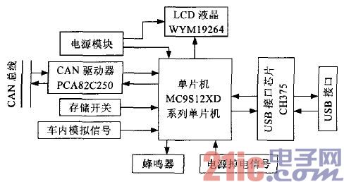
Figure 1 System overall structure
2 system hardware design
According to the overall structure of the system, the hardware circuit mainly has the following major modules: main controller module, liquid crystal module, CAN driver module, power module, CH375 interface circuit module.
2.1 main controller module
The system CPU uses the MC9S12XD series of single-chip microcomputers from Freescale. It is the core of the control and communication part, not only responsible for system initialization settings and message reception, but also related data judgment processing and display. The chip integrates almost all analog and digital peripherals and other functional components required to form a microcontroller control system and data acquisition system. The main features are as follows:
(1) The MC9S12XD series has a unique XGATE coprocessor. The CAN signal reception in this system is completed by the interrupt program, and the interrupt handler is handed over to XGATE for processing, which will reduce the CPU load and improve the system's response speed.
(2) With l6 analog-to-digital conversion channels, it provides hardware support for acquiring analog signals, and can be programmed to be accurate to 10-bit precision.
(3) With 5 MSCAN modules, the CAN controller is integrated internally. The configuration of the CAN module is essentially converted into the configuration of the corresponding registers of the MCU, which is convenient and flexible to use.
(4) Background debugging mode BDM support makes the debugging of the chip extremely convenient and speeds up the product development cycle.
(5) A rich source of interrupts provides sufficient protection for the system to operate under non-operating system support.
2.2 LCD module
The system uses WYM19264 LCD, which is divided into 3 screens, and each screen can display a dot matrix with a capacity of 64x64. The liquid crystal external interface adopts a 20-pin pin socket, and the connection circuit with the single chip microcomputer is also relatively simple, wherein the chip select signals CS1 and CS2 are respectively connected with the PH6 and PH5 of the single chip microcomputer, and the control signals RS, R/W, EN are respectively associated with PK4 and PJ1. PJ0 is connected, and 8 data lines (DBO~DB7) are connected to the 8 pins (PB0-PB7) of the PB port for parallel port transmission.
2.3 CAN driver module
The CAN driver interface chip uses PAC82C250, which is the interface between the CAN protocol controller and the physical bus. It is mainly designed for high-speed communication (up to 1Mbps) applications in automobiles. This device provides differential transmit capability to the bus, differential transmit capability to the CAN controller, and protection against transients in the automotive environment to protect the bus. Its pin 8 (Rs) allows to select different operating modes: high speed, standby, and slope control. In this system, the pin 8 is grounded and its high speed mode is selected. RX and TX are connected to the pin of the single-chip CAN module. In this system, the CAN0 module is selected, that is, connected to RXCAN0 and TXCAN0 respectively.
2.4 Power Module
The power of the recorder is taken from the 12V vehicle battery power supply. In addition to the system operation, the power supply is also responsible for the power supply of ignition, lighting, signal and other equipment. The power supply fluctuates greatly and the interference is serious. Because the car is in the process of driving, it may encounter road surface comparison. In the worst case, the power supply interface of the recorder may be loose or poorly contacted due to severe vibration, so the power module must be carefully designed to meet the demand.
The schematic diagram of the power module circuit is shown in Figure 2, where U1 is the 6V backup power supply provided by the battery, U2 (main power supply) is the vehicle 12V power supply, the power supply module is divided into 2 channels, and the +5v voltage is stabilized by the 7805 voltage. Power is supplied to the liquid crystal, and the VCC converted by 4275 supplies power to the entire single chip and the auxiliary circuit. When the system is working normally, D1 is in the off state, and the backup battery does not work. Once the main power supply is lost, D1 is turned on quickly, and the backup power supply automatically starts to supply power to the system.
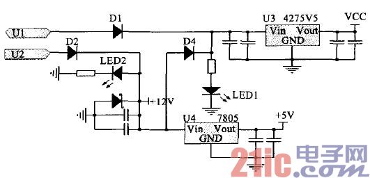
Figure 2 Power Module
There are two reasons for this design of the power module, as shown below:
(1) The use of backup batteries. The recorder stores the collected data, and the collected data is sequentially written into the cluster allocated for the record file. When the acquisition ends, the experimenter disconnects the storage switch or the collection is forced to terminate due to the power failure, and the single-chip microcomputer needs to close the record file. An important deal. Closing a file means writing the actual length of the file and the total number of records collected into the file header. If the file is not closed properly, or because the power is too late to close the file, Windows will not be able to find the end of the file, and the PC software will not be able to open the file because it cannot find the end of the collected data. At this time, the collection work will fail. . In order to prevent the file from being closed due to power failure, the system uses a spare battery.
(2) The single chip and the liquid crystal are separately powered. When the main power supply works normally, the power of the whole system is supplied by the main power supply. Once the main power supply is powered off, the backup battery only supplies power to the single chip microcomputer, and the MCU completes the file processing, and the liquid crystal does not work due to power failure. Due to the large power consumption of the liquid crystal and the limited backup battery power, this separate 2-way power supply method not only provides the power supply for closing the file, but also saves battery power.
Of course, the backup battery cannot be used for a long time, and can only be used for system emergency shutdown file processing. For this purpose, a power detection signal is designed. Once the main power supply is detected, the buzzer and the light-emitting diode are enabled to remind the user that the power supply is not supplied. Normal, the staff is required to check the recorder power connector.
2.5 CI-I375 interface circuit module
The USB interface chip in this system is selected from CH375 of Nanjing Yuheng Electronics Co., Ltd. The chip supports host mode and device mode. It has 8-bit data bus and read, write, chip select control lines and interrupt output, which can be easily hooked up. Go to the system bus of the microcontroller. It also has built-in firmware for handling the dedicated communication protocol of the Mass-Storage mass storage device. The external MCU can read and write the U disk directly in the sector as the basic unit.
The read strobe signal RD#, the write strobe signal WR#, and the chip select signal CS# are both input signals and active low, CS# is the interrupt request output signal, and is also active low. The A0 signal is used to distinguish between commands and data. When A0=1, the command can be written. When A0=0, the data can be read and written. The 8-bit bidirectional data bus is connected to the PA port (PA0-PA7) of the MCU, and the parallel port is transmitted. The hardware supports automatic detection of the USB device connection function. When the host mode is normally connected, the ACT# pin outputs a low level. Therefore, the ACT# I pin is externally connected with a pull-up resistor and connected in series with an LED to indicate whether the USB device is connected. Normal connection.
When laying the PCB, try to make the 7805 chip on the edge of the board and the heat dissipation is better, and away from the LCD screen. Because in the actual process, after testing, the 7805 chip generates a lot of heat, if used for a long time and close to the LCD screen, it will affect the display effect of the liquid crystal. In addition, try to make the LED of the power module close to the power interface. The LED of the USB module is close to the USB module and is separated by color to facilitate user observation.
3 system software design
In the software design, the modular design idea and the interrupt calling scheme are adopted. After the system is powered on, the system first initializes, and the information on the CAN bus is received by the interrupt mode. The interrupt program is processed by XGATE, and the system generates an interrupt every time one frame is received. To trigger the microprocessor to enter the interrupt, read the frame data in the interrupt service routine and temporarily stored in the cache. This cache is shared between XGATE and CPU. Since the data unit of reading and writing u disk through CH375 is one sector, the system sets the cache to one sector (512 bytes). When the cache is full, the data is dumped by the main program. Go to the U disk.
The main functional modules of the system software part include: main program module, initialization module, and interrupt processing module.
3.1 main program design
The main program flow chart is shown in Figure 3.
As can be seen from the flow chart 3, during the entire program operation, a query is used to detect whether the power supply is powered down. Since the CAN signal transmission frequency in the car is several tens of milliseconds, if the LCD screen displays the data in real time, the screen refreshes too fast and is not easy to observe. Therefore, the system setting refreshes the screen data when the buffer is full, such that the refresh frequency is sufficient. To meet the needs of users, the LCD screen provides display services regardless of whether the memory switch is closed or not. Sudden power loss during recording or user disconnection of the memory switch will cause the current recorded file to be closed, that is, modify the file pointer and file length and other file system related processing.
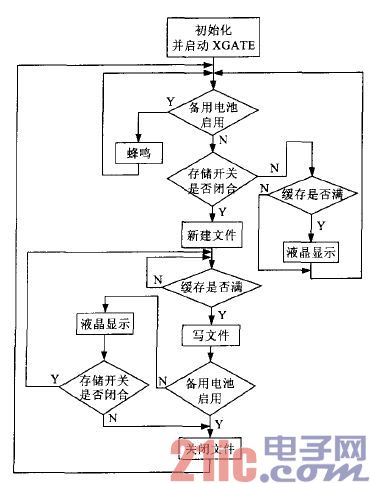
Figure 3 main program flow
3.2 Initialization module
(1) Initialization of the CAN module
The initialization design of the CAN controller is the key point. Each register written must be carefully and comprehensively considered. If the initialization is not successful, the system will not work properly. This recorder essentially participates in communication as an add-on node of the entire CAN network, and all CAN nodes in the network must be synchronized. To initialize the CAN module, you must first enter the initialization mode, initiate the request by setting the IN-ITRQ (CANCTLO) bit, and get the response from INITAK (CANCTL1), the MSCAN enters the initialization mode. In this mode, registers such as CAN-BTR0, CANBTR1, CANIDAR, and CANIDMR are usually configured. CANBTR0 determines the value of the baud rate prescaler and the sync jump width. CAN_BTR1 determines the width of the period, the position of the sample point, and the number of samples at each sample point. The appropriate value is set according to the specific CAN bus communication rate. CANIDAR and CANIDMR jointly determine which ID frames need to be received. In this system, the purpose of the CAN bus recorder is to receive all the messages of the CAN line data, thus setting the CANIDMR to 0xFFh, that is, all bits are not masked, and all frames are received. After setting the registers to be configured, you need to exit the initialization mode and participate in CAN bus communication.
(2) Initialization of CH375
Mainly set the USB working mode, set the working mode code to 06H through the SETUSB MODE command provided by CH375, that is, in the USB host mode, it automatically detects whether the USB device is connected. When the USB device is connected or disconnected, an interrupt will be generated to notify the external device. The MCU, and automatically generates a USB frame period start packet SOF is sent to the connected USB device. Normally, the USB working mode is set to be completed in 20 microseconds, and the operating state is output after completion. Obtain the operation status by reading the PA port to check whether the setting is successful. If it is unsuccessful, it indicates that the CH375 is faulty. For example, if the chip model is wrong or is in the serial port mode or is not supported, the u disk cannot be read or written.
3.3 Interrupt Processing Module
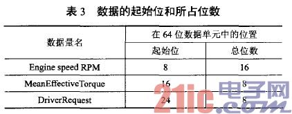
The interrupt module accepts the interrupt. Since all the frames of the system are set to be received, the received frame must be judged in the interrupt processing function and "decoded". The process of "decoding" is described in detail with examples. As shown in Table 1, two important CAN messages in the A5 car are listed. The IDs are in the standard format (11 bits), and the data units occupy 64 bits (8 words). Section). After receiving the data frame, the ID number is first taken. For the standard frame format, IDRO stores IDIO~ID3, and the upper 3 bits of IDR1 store ID2~ID0, so ID number=(IDR0<<3) l (IDRI>>5), where the ID number is set to an int variable. After the ID number is obtained, the message will be decoded according to the message list. For example, if the obtained ID number is 0xFA, this is the message frame from the engine control unit EMS (engine management system), we will take out the 64-bit data unit from it. The data of interest, in which the 64-bit data is stored in the result registers DSR0-DSR7, is shown in Table 2. Suppose we take the following three data from this frame: Engine speedRPM, MeanEfectiveTorque, DriveRequest.
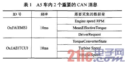
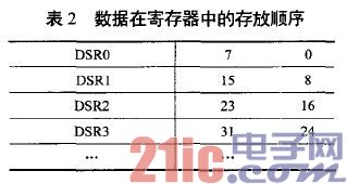
Table 3 lists their starting bits and their number of bits in a 64-bit data unit. Here is a little explanation of the Engine speed RPM with 16 bits of data. Since the selected microcontroller uses the Motorola big-end mode, the lowest bit is the 8th bit in DSR1, not the 0th bit in DSR0. Our upper PC data analysis software is in Intel format, so we need to convert the multi-byte data to the big end. The following gives an example of a function statement:
Engine speed RPM DSR1;
Engine speed RPM = (Engine speed RPM<<8) IDSR0;
M eanEfectiveTorque=DSR2;
DriverRequest=DSR3;
For multi-byte data, size-to-edge conversion is required, while single-byte data is directly copied. Store the collected data in the cache and then end the interrupt.
3.4 Other modules
The liquid crystal module uses "prefabricated screen" for the part that needs to be fixedly displayed to reduce the burden and repetitive work of communication transmission during work. Read and write u disk module, the data in u disk is stored in file format, MCU read and write u disk is mainly based on FAT file system for various operations of files and directories, CH375 provides u disk file level subroutine library This library supports FAT16 and FAT32 file systems. Users only need to call various API functions of this library to read and write data blocks. A/D conversion module, the configuration of control register 5 (ATDCTL5) should be cautious, because the write operation of this register will interrupt the current analog-to-digital conversion sequence and start a new conversion sequence. It is recommended to put this register in the first 4 controls. Configured after the register.
4 Conclusion
The driving recorder developed by this system has been successfully applied to various road tests such as 30,000 kilometers and 50,000 kilometers of A5 vehicles, accurately recording important data during the driving process, performing performance analysis, fault analysis, and research for researchers. Calibration work provides an important data basis. Using a CAN-based driving recorder on a vehicle with a CAN bus can significantly reduce system complexity and reduce costs. For different models, only a small modification of the software without the need to change the hardware makes the recorder extremely flexible and portable, so it can be widely used in various models.
SAMSUNG Cylinder , original and new, in stock.
The cyclinder for SAMSUNG SMT Machine has J67010088B, HP03-900013, CM2C32-50Z-XC, J67011047A
All the products will be checked before delivery.
Ejector For Vacuum
Smt Vacuum Ejector
Smt Vacuum Valve
Samsung Cylinder
Panasonic Pir Sensor
Panasonic Sunx Sensor
Panasonic Original Sensor
Panasonic Sensor
SAMSUNG Cylinder
Samsung Cylinder,Samsung Air Cylinder,Cylinder For Samsung,Smt Samsung Cylinder
Shenzhen Srisung Technology Co.,Limited , https://www.sr-smt.com