But the current trend is in the opposite direction: the functions of mobile phones are constantly increasing. It currently includes Internet access, audio, video, and multi-mode capabilities with voice and data, all of which have increased battery consumption and reduced runtime. To meet market requirements, mobile phone designers have developed mobile phones that support many capabilities and multiple standards, including GSM, CDMA, Wi-Fi, HSDPA, WCDMA, etc. on one mobile phone. However, the increase in functions increases the required driving power. Even if some functions are not running, power consumption is required. In earlier mobile phone designs, power consumption was mainly determined by the RF power amplifier, microprocessor, backlight, and display. Designers have made many efforts to reduce power consumption on these subsystems, so that the absolute power consumption during operation is reduced to the smallest possible level. Although the battery is also constantly improving, but it can not keep up with the development requirements. In order to make mobile phones smaller, thinner and lighter, a battery pack with a smaller size and weight is required, and it is necessary to meet the requirements of a larger display screen, more functions and longer battery life. To meet these requirements, in addition to tapping as much potential as possible in traditional areas, mobile phone designers must also reduce power consumption as much as possible. Today, mobile phone designers have turned to dynamic power consumption methods that can significantly reduce power consumption. With this new technology that saves power, the subsystems in the phone will be turned on or off as needed. But these subsystems are always connected to the internal power cord of the mobile phone, and even when disabled, they will leak power. In order to support many RF standards and functions required by users, the number of these subsystems is still rising. Although the power consumption of each subsystem when it is disabled is small, it will consume a considerable amount of battery power when added together. Modern mobile phones use 20 different voltage regulators to optimize the performance and power consumption of each subsystem. And many levels make the problem more serious. In the R & D laboratory, engineers need to make a lot of hard work to make changes to the mobile phone software and hardware to minimize current leakage and optimize battery life, even if such changes are usually very small. They must accurately assess the total current consumption of the phone in the laboratory, and independently measure the current when each subsystem is turned on or off to understand its impact on the overall design. Current popular solutions Although most of the power supplies used to power mobile phones in the test have built-in current measurement capabilities, these measurement results may not be accurate enough. If the power supply cannot measure current at the μA level, the ATE system designer will switch to a digital multimeter. But when using a digital multimeter to measure the μA level current, the power path passes from the power supply through the digital multimeter to the DUT. This will increase the complexity and noise of wiring. When multiple DUTs need to be tested in parallel, using a digital multimeter means adding multiple switches and increasing the test time to wait for the switches to stabilize and measure multiple DUTs in sequence. To improve the system throughput, each DUT can be equipped with a digital multimeter, which naturally increases the cost and complexity. Another way to measure these dynamic currents is to use a dedicated power supply that can only be provided by a few ATE manufacturers. This type of power supply uses a high-bandwidth voltage regulator and an integrated digital current measurement system that can measure a wide range of currents. During the test, the dedicated power supply is used to replace the battery of the mobile phone. The power supply can measure the current flowing into the mobile phone during the test and directly give the power consumption and leakage current of the mobile phone. Mobile phone manufacturers use such dedicated power supplies in production tests to verify that mobile phones can meet power requirements. This type of special power supply can also be used to characterize mobile phones and their key components in the laboratory. In the production of mobile phones, most manufacturers will measure various working states of mobile phones, such as the large current when sending, receiving, playing and accessing the Internet, and the small current when shutting down or standby. High current measurement can maintain the fast throughput rate of ATE system, but measuring small current is generally slower, because the standby mode, sleep mode and leakage current measurement require a long integration period to eliminate noise. It should be noted that the mobile phone is switched between high current leakage (such as during a pulse transmission) and low current leakage (such as when on standby). This requires the power supply to be like the battery of a mobile phone. The power supply must have a fast transient response capability to ensure voltage stability. If the power supply causes fluctuations in the power supply voltage of the mobile phone during transient changes, the low battery voltage detection circuit of the mobile phone may turn off the mobile phone. In order to accurately measure the extremely low current flowing from the battery, these power supplies have high resistance current shunts (100Ω to 10kΩ). A large uncorrected shunt resistor will cause a very large drop in the output voltage, as well as the instability caused by the capacitive load common in DUT bypass networks. For this reason, these power supplies must dynamically short-circuit these high-resistance shunts with dedicated circuits to improve the transient response of the power supply to an acceptable level. Many specialized power supply manufacturers have their own technologies, many of which are protected by patents. Shortcomings of current solutions In this type of technology, in order to solve the stability problem, a large capacitor is often connected to a high resistance shunt. Although this solves the voltage stability problem, it will waste a lot of measurement time. Because when a small current flows through these large resistance shunts, the combination of a large resistor and a large capacitor forms a high time constant and a longer settling time. In addition, these technologies also use MOSFETs to connect large resistors to short-circuit the resistors and capacitors when driven at high currents. Excitation of these FETs will produce a discontinuous output voltage, which is a difficult challenge to overcome, and not all manufacturers' products will be successful. Most solutions use these technologies to provide sufficient performance for the final test of the mobile phone, but whether it is in the measurement speed or in the dynamic measurement range, it still cannot meet the requirements of measuring various components in the mobile phone. The current test of the mobile phone production test system usually needs to complete the measurement accuracy of 30μA within 100ms. But this is too slow and inaccurate for testing semiconductor devices in mobile phones. Semiconductor devices require faster testing, and the operating current is much smaller. Many devices even require sub-μA measurement accuracy and tens of milliseconds measurement speed. Patented technology for low current measurement In order to measure these low-level currents faster and more accurately, Agilent designers clearly realize that it is impossible to meet the end user requirements by developing the above technology alone. There is now a new method for accurately measuring low current based on Agilent's patented technology. The Agilent power supply using this patented technology has a fast transient response at high current, and can perform fast and accurate low-level current measurement. This power supply can make faster small current measurements because it does not need to wait for the internal large capacitor to charge and the signal to stabilize. It can complete μA-level current measurement within a few milliseconds, and the error is less than 100nA. For currents greater than 2A, the transient response time is less than 50μs. Agilent's patented solution uses an active method, which removes the capacitor connected to the current shunt in the current solution. Although there is no capacitor, this active method still solves the instability problem caused by the large-value shunt. Without capacitors, a faster response time is achieved. The patented circuit uses an operational amplifier to reduce the resistance (usually 10kΩ or higher) of the large-value shunt in the power supply output path to only a few mΩ. If the current flowing through the op amp exceeds the maximum threshold, it turns on a set of MOSFETs, allowing a higher current to flow through a large resistance shunt. The switching of these MOSFETs is done in a seamless manner without generating any voltage discontinuities. This technology allows faster low-level current measurements while retaining excellent transient response performance for today's dynamic loads. Application areas of patent solutions Mobile phone manufacturers can use this solution in production test systems to accurately measure the overall power consumption in standby mode. Mobile phone component manufacturers, such as microprocessors, RF power amplifiers, and other related circuit manufacturers can also use this solution in their production test systems. By using the power supply to quickly measure low current, the manufacturing test system does not need to wait for the current measurement result, thereby improving the throughput of the test system. When characterizing the transmission characteristics of a mobile phone's power amplifier, throughput is critical to make the most of expensive RF test resources. Whether it is for robots or component production lines, the equipment footprint is also an important factor. High throughput and small equipment size are conducive to the efficient use of existing plant space, conveyor belts, and RF test equipment. The DC output module (Figure 1) of the Agilent N6700 modular power supply has adopted these new measurement techniques. R & D and production line engineers can configure a set of 1-4 output DC power systems by selecting 22 DC output modules with different power, voltage, and performance levels. Agilent provides the N6705A DC source analyzer for R & D applications (Figure 2), which is a brand-new test instrument that integrates 4 power supplies, digital multimeter, high-power arbitrary waveform generator, oscilloscope, and data logger into one instrument The volume is also suitable for use on the workbench. The DC source analyzer has a full-featured and friendly user interface, can quickly set up the test, and does not require programming. For manufacturing, the Agilent N6700 1U highly modular power supply system provides ATE system designers with the flexibility to optimize performance, power, and price to meet production line testing needs. The N6700 modular power system has three mainframes, 400W-1200W, and 4 modules can be installed in a 1U high chassis, thus increasing the density of the DC power supply to the maximum. When using the module equipped with the option 1UA μA-level current measurement system in the N6700 modular power system host, the measurement characteristics include integrating the μA-level current measurement through its built-in ammeter and capturing the data to 50kHz digitizer 4096 point buffer. When the N6705A DC source analyzer is installed in the power supply module with option 1UA, the μA class current measurement system can capture the current using the DC source analyzer's built-in ammeter, oscilloscope, and data logger function. In addition to measuring low current, Option 1UA also adds a mechanical relay to disconnect the positive and negative sides of the power supply, including the remote sensing line, so as to achieve complete electrical isolation between the power supply and the device under test.
HV Bus Bar Insulator is mainly made from bulk molding compound, unsaturated polymer with fiber glass. Bus bar composion insulator are with good properties such as electrical resistance, hear resistance, fire resistance,electrical Bus Bar Insulator is low shrinkage and water resistance. Bus Bar Suspension Insulator description is as follows:
Electrical Bus Bar Insulators,Bus Bar Suspension Insulator,Bus Bar Composite Insulator,Hv Bus Bar Insulator FUZHOU SINGREE IMP.& EXP.CO.,LTD. , https://www.cninsulators.com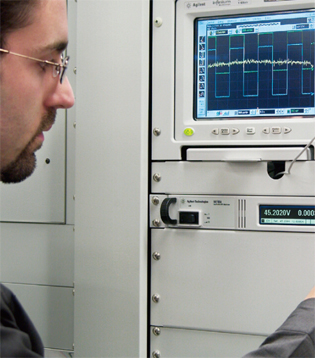
Figure 1: The IU-height Agilent N6700 modular power supply is an ideal device for automated test systems. 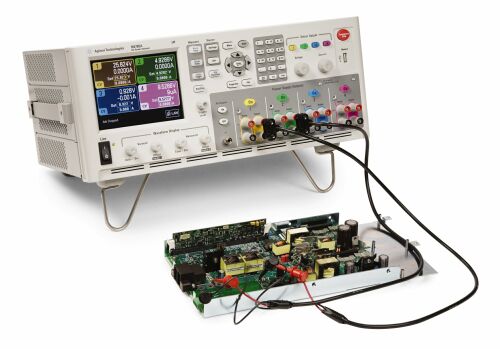
Figure 2: An Agilent N6705A DC source analyzer tailored for R & D engineers.
But inserts: Brass, various specifications are available
Test specifications: JIS C3801 and JIS C3851
Color: Dark brown or dark red

")


We warmly welcome friends both domestic and abroad to visit our company, if you have any questions, please contact with us directly.
In the mobile phone market, cell phone battery life is a technical indicator that any customer can easily assess. Insufficient battery life will cause user dissatisfaction. Therefore, when designing mobile phones and their key components, extending battery life by reducing power consumption is an important design consideration.