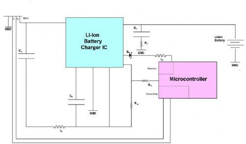
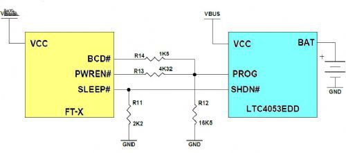
USB is more convenient for a variety of portable devices by means of a single "universal" power supply. But there are also many challenges in this regard. Previous USB charging capabilities were quite limited; the current on a standard USB host port was really only suitable for powering computer peripherals such as keyboards, mice, and card readers. USB 2.0 supports a supply current of up to 500mA, which can slowly charge the battery. At the same time, what everyone is looking forward to is how to significantly shorten the charging time. In this environment, the 1.2 version of the USB charging specification introduced in early 2011 proposed a new power supply mode, which increased the flexibility of charging the device battery. This article describes the concept of a dedicated charging interface (DCP) that can support up to 1.8A. This is almost four times the current carrying capacity of the standard downstream port (SDP) USB 2.0 connection, which greatly speeds up the charging time. About DCP The USB interface has 4 shielded wires. They are: VBUS for powering the connected peripherals, negative data terminal D-, positive data terminal D+, and ground GND (Figure 1). In DCP, D+ and D- are shorted together by a 200Ω resistor to prevent data transfer. It indicates to the connected peripheral that the port is fully focused on the charging function and does not provide a master function. Any portable device connected via a USB port can distinguish whether it is in DCP or SDP. This allows it to take advantage of the larger available charging current. Figure 1: Differences between DCP and SDP Figure 2: Traditional USB Battery Charging Line FTDI is committed to simplifying USB charging to minimize development time, system complexity and engineering resources for maximum return on investment. This led to the X-CHIP series of USB controller ICs, the main feature is to support the new concept of USB battery charging. The internal circuitry of each IC enables a portable device designed with this chip to detect when the device is connected to the DCP. Once the DCP is detected, X-CHIP sends a signal on one of its CBUS pins to initiate charging. Figure 3 depicts an X-CHIP based battery charging application. The circuit charges the battery when it is connected to a USB host port or DCP. The CBUS pin can be used to control the battery charge rate (depending on the power supply detected and the corresponding current limit). The battery charge rate is determined by the resistance of the PROG pin connected to the Linear Battery Charge Controller LTC4053. Figure 3: Simplified USB charging line The CBUS pins include BCD#, PWREN#, and SLEEP#. BCD# is an open-drain active low output signal. It is used to indicate when X-CHIP is connected to the DCP. PWREN# is an open-drain active low output signal. It shows that X-CHIP has been enumerated by the USB host controller. This signal is used to select the value of the resistor on the PROG pin to drive a 500mA charge. SLEEP# is a push-pull active low output signal. It shows when X-CHIP enters USB suspend mode. This signal is used to power off the LTC4053 when the device is powered by the USB host and the host sets X-CHIP to suspend mode. In Figure 3, the impedance of the PROG pin of the LT4053 is set by resistors R12, R13 and R14. BCD# is used to configure the resistor network of the PROG pin to achieve a charging current of approximately 1A. The BCD#, PWREN# and SLEEP# outputs are designed to minimize the external circuitry of the charging application. Typically, external MOSFET devices require a range of choices. As mentioned earlier, X-CHIP drives the BCD# signal to indicate the detection of the DCP. The open-drain output shorts R14 to ground, so the impedance of the LTC4053 PROG pin will be 16.5k? With 1.5k? The resistor is connected in parallel to ground. This can trigger a charging current of nearly 1A. When X-CHIP is connected to a standard USB host controller, this pin is not driven and the device operates as a traditional USB interface chip. Since the BCD# signal is an open-drain output with no internal pull-up, it can be used to pull resistor R14 down to ground without the need for any external MOSFET. When the device boots, the CBUS pin defaults to input and has a weak pull-up until the MTP ROM is read. This will take approximately 14ms, after which the CBUS pins will take their chosen function and work as described in this article. Summary of this article Thanks to the wide application of USB, the USB port is clearly a convenient place for portable devices to obtain power. By separate interconnection, 10W power can be supplied to a variety of different devices. Moreover, the implementation of USB charging standardization in countries (including China and EU member states) enables consumers to use fewer charging cables. This will increase the number of e-wastes entering the environment each year while increasing convenience (this is mainly due to custom adapters). By using an integrated approach rather than relying on discrete devices, you can create better charging circuits for space, device, and engineering resources. USB is not only the most popular digital interconnect, but also a key system component for electronics power and battery charging. Plate Non-damaged Desulfator with Smart Pulse, Smart Restorer with Battery Charging Ability. Battery Charger And Restorer 2-in-1 Battery Charger And Restorer 2-in-1,Battery Charger Restorer,Battery Smart Charger and Restorer,External Battery Smart Charger Shenzhen Daceen Technology Co., Ltd. , https://www.daceen-sz.com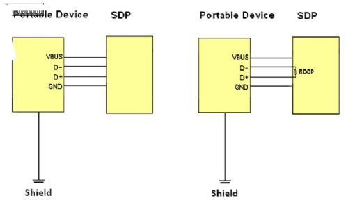
When the lead-acid battery is under using or stored status for a long time, due to factors such as undercharge, self-discharge and environmental temperature changed, its performance will gradually decline, and it might even not be used any more. The main cause of battery failure is that the lead sulfate on battery plate gradually lose activity for the above factors. The crystallization thickens and hardens, cannot be reduced to fluffy lead as recharging, as a result, the battery capacity decreases or to be completely scrapped. This phenomenon is known as [irreversible sulfation".
Battery Charger and Restorer 2-in-1 is a multiple-stage charger with smart pulse maintenance ability. It is a Battery Desulfation Charger with a Automatic battery maintainer's function. This innovative, state-of-the-art battery restorer smartly knows how to restore battery in charging process, Unlike other common chargers on the market, you don't need to select the battery type. It works smartly on any type of 12/24/36/48/60/72-Volt lead-acid battery – VRLA, AGM and Flooded. Proprietary algorithms combined with microprocessor & IC controlled technology measure the battery's voltage and current to automatically determine and deliver the precise pulse frequency and duty cycle based on the size and condition of the individual battery.
Battery Charger And Restorer 2-in-1 is more than a common pulse charger and desulfator. It is a multiple-stage pulse charger with Optimizer and Recover, During the restorative battery charging cycle, VoltaTech's patented, optimized High-frequency pulsing and smartly changeable duty cycle constantly work to minimize and reduce battery sulfation and internal resistance. By reducing the size and number of lead sulfate deposits on the battery plates- the No.1 cause of battery failures, increase capacity and release energy to keep battery in new conditions, your battery will charge deeper, maintain greater reserve capacity and last longer service lifespan– up to 2 times longer.
To reduce the charging links of the battery to be stored, after removal from various military equipment and Military backup power(UPS), the batteries can be directly connected to our smart lead-acid battery emergency support system, which can smartly enter pulse maintenance state after fully charging the battery,The tiny pulse charging current can also offset the self-discharge of battery, and ensure that the battery can be put into emergency use at any time no matter how long it is stored.