EDA (Elect rONic Design AutomaTIon) is an electronic design automation technology that refers to the integration of application electronics, computer technology, and intelligent technology into a common electronic software package using computer as the basic working platform to assist in electronic design of three aspects. Work, namely integrated circuit design, electronic circuit design, and PCB design. In summary, the basic feature of EDA technology is the use of high-level language descriptions with system simulation and synthesis capabilities. It generally uses a top-down modular design approach. However, due to the size of the digital system designed and the complex logic relationship within the system, how to divide the logic function module becomes the most important task of designing the digital system.
Introduction to MAX+ plus II
MAX + plus II is a structure-independent, fully integrated design environment that allows designers to easily design input, fast processing, and device programming for Altera's various CPLD families. The MAX+ plus II development system offers powerful processing power and a high degree of flexibility. Its main advantages: structure-independent, multi-platform, rich design library, open interface, fully integrated, support for multiple hardware description languages ​​(HDL).
Design Flow
The design of the digital system adopts a top-down, coarse-to-fine, and step-by-step decomposition design method. The top-level circuit refers to the overall requirements of the system, and the bottom layer is the implementation of a specific logic circuit. The top-down design method gradually decomposes a complex system into several functional modules for design description, and uses the EDA software platform to automatically complete the logic synthesis and optimization of each functional module, the layout of the gate-level circuit, and then download to the hardware. Implement the design. The general flow of circuit design using MAX + plus II is shown in Figure 1.

The specific design process is as follows.
1) Design input. MAX + plus II supports a variety of design input methods such as schematic input, waveform input, text input, and their mixed inputs.
2) Design processing. After the design is input, compile, check, and modify with the MAX + plus II compiler until the design input is correct. At the same time, the input file is logically simplified and optimized, and finally a programming file is generated. This is the core of the design.
3) Design inspection. MAX + plus II provides designers with a comprehensive inspection methodology for design simulation and timing analysis. The purpose is to verify that the logic function of the circuit is correct and to test the worst-case delay of the target device. This troubleshooting process is critical to verifying the competitive risk of combinatorial logic circuits and the timing, delay, etc. of sequential logic circuits.
4) Device programming. After circuit design and verification, the MAX+plus II Programmer downloads the compiled files generated by the compiler into a specific CPLD device, which implements the physical programming of the target device.
Design a modulo 60 counter with text input method and graphic input method
System analysis
The modulo 60 counter can consist of a decimal counter and an asynchronous clear hex counter. This design consists of a decimal counter 74160 component and a hex counter. After the digital system is partitioned, you need to choose the way to correctly describe the logical functions of the system. For the selected CPLD, you need to use the corresponding design development software. For example, the design description of MAX + plus II has various ways of text, waveform and graphic. Graphic input is intuitive and easy to understand. When the system is large, it is very inconvenient to use because there are many connections in this way. The description of the V HDL hardware description language is independent of the structure, the design difficulty is reduced, the software modification is convenient, and most of the controlled function modules have been compiled and verified. When the system is designed, these modules can be selected and combined according to certain logic functions.
system design
The design hex counter is designed with text input. The code is as follows:
L IBRARY ieee ;
USE ieee. STd_LOGIC_1164. all ;
USE ieee. std_logic_unsigned. all ;
ENTITY counter6 IS % defines module IS
PORT (Load , En Clrn , Clk : IN STD_LOGIC;
D : IN STD_LOGIC_VECTOR(2 downto 0) ;
% defines the input port
Q : OU T STD_LOGIC_VECTOR (2 downto 0) ;
% defines the output port
Co :OU T STD_LOGIC)
END counter6 ;
ARCHITECTURE a OF counter6 IS
BEGIN % definition process
PROCESS(Clk)
Variable tmp : std_logic_vector (2 downto 0) ;
% defines a vector
Begin
IF Clrn = '0'THEN tmp : = "000" ;
Else
IF ( Clk'event AND Clk = '1') THEN % process statement
IF Load = '0'THEN tmp : = D ;
ELSIF En = '1'THEN
IF tmp = "101" THEN tmp : = "000" ;
ELSE tmp : = tmp + 1 ;
END IF ;
END IF ;
END IF ;
END IF ;
Q < = tmp ; Co < = (tmp (0) AND tmp (2) AND En) ;
END PROCESS ;
END a ;
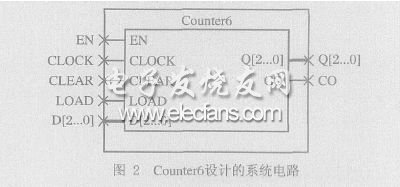
Save and compile the design code, then create the circuit symbol counter6, then edit the modulo 60 counter with graphical input, and reference the hexadecimal circuit symbol counter6 during the editing process. The system circuit designed is shown in Figure 2.
The modulo 60 counter consists of a decimal counter 74160 and a hexadecimal counter designed as above (see Figure 3). When the 74160 counts to 9, a carry is generated to enable the hex circuit to count.

System Simulation
In order to ensure the correctness of the design, the system is designed to be simulated. This system uses MAX7000S series CPLD chip, and uses MAX+plus II to compile various files from bottom to top, and then perform logic simulation. The simulation waveform is shown in Figure 4. After the simulation, the MAX + plus II Programmer is downloaded to the programmable chip to complete the design. Compile and debug with MAX + plusII to generate a counter that can implement modulo 60. From Figure 4, the initial value is 58, the enable terminal EN and the clear control terminal CL RN are high. After two clock cycles rising edge Qa changes from 8 to 0, Qb changes from 5 to 0, and then starts a new round of counting.
Conclusion
The digital circuit system design uses advanced EDA software and hardware description language, and realizes design by means of CPLD, which embodies the digital circuit design system chip. The systematic design of the chip makes it easy for designers to construct digital integrated circuits based on their actual needs.
Even you are troubling in powerless headphones and mobile phones, Power Bank Bluetooth Earphone help solve this problem. This power bank Bluetooth Earphone is not only Bluetooth earphone, also own emergency power bank, keep the longer life of earphone and mobile phone.
With the continuous development of modern society, more and more communication equipment now become people's daily portable products. More and more functions are required, and the demand for volume and quantity is less and less. Therefore, we also launched a new X4T, in the original Bluetooth function based on the addition of wireless and mobile power supply functions, 5200mAH power bank and wireless charging battery can give your mobile phone and other modern communications equipment complete 1-2 full charging, provide your intelligent life convenience.
Power Bank Bluetooth Earphone
Power Bank Bluetooth Earphone,Bluetooth Earphone With Power Bank,Power Bank With Bluetooth Earphone,Portable Power Bank With Bluetooth Earphone
ShenDaDian(China) Digital Electronics Co.,Ltd , http://www.btearbuds.com