This paper introduces the design and implementation method of all-digital single-phase inverter based on DSPTMS320LF2407A and using SPWM control technology. Finally, the experimental waveform is given.
Common AC/DC/AC inverters are frequency conversion and variable voltage regulation of the output part, and among the various inverter control technologies, one of the most widely used inverter control technologies is sinusoidal pulse width modulation (SPWM) technology. . In the variable frequency speed control system, DSP is used as the control chip to realize digital control. It not only improves the system reliability, but also makes the system control precision, real-time strong, simple hardware, easy software programming, and is a variable frequency speed control system. One of the most promising research directions.
Introduction to TMS320LF2407A chip
The TMS320LF2407A is a monolithic DSP controller designed by TI for motor control. It has a high-performance C2XLP core, improved Harvard architecture, and four-stage pipeline operation. It not only has powerful high-speed computing power, but also integrates a wealth of motor control peripheral components, such as event manager EVA and EVB. Independent bidirectional timer; supports programmable dead-time control PWM output; 2 of the 4 capture ports can directly connect quadrature-encoded pulses from the opto-electronic encoder; 2 independent 10-bit 8-channel A/D converters The conversion of two analog inputs can be completed in parallel at the same time; the on-chip serial communication interface can be used to communicate with the host computer; the on-chip serial peripheral port is used for communication with the peripheral; 40 independently programmable multiplexing I The /O port can be selected as an input/output port for keyboard input and oscilloscope display. These provide great convenience for realizing variable frequency speed control of AC motors.
System overall scheme and hardware circuit
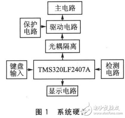
Figure 1 shows the hardware block diagram of the system. In this system, TMS320LF2407A is the main control chip, and the inverter adopts SPWM modulation control method to realize the frequency conversion control algorithm. The system hardware consists of main circuit, display circuit, keyboard input circuit and detection and protection circuit. The DSP first collects the required frequency signal from the keyboard, and then generates a corresponding SPWM signal through the operation, transmits the optical tube to the driving circuit through the optical coupling, and then controls the power tube in the inverter bridge to be turned on and off, and simultaneously acquires relevant signals in the main circuit. Determine if there is a fault output. If there is a fault, turn off the SPWM output of the DSP, thus turning off the main circuit.
1, the main circuit composition
Figure 2 shows the main circuit of the system, which consists of a rectifier circuit, a filter circuit and an inverter circuit. The rectifier circuit is a three-phase uncontrolled rectifier bridge, which converts 380 V, 50 Hz AC power into pulsating DC power. Filtering capacitors are used in the circuit to filter out the voltage ripple, and the filter capacitor is also decoupled between the rectifier circuit and the inverter to eliminate mutual interference. The average value of the rectified DC voltage is UO=1.35U2≈1.4U2=540 V. U2 is the rms voltage rms value. Considering that the input three-phase power has a 10% fluctuation, UO=500~560 V. The power devices G1, G2, G3, and G4 in the main circuit diagram indicate IGBT devices, the model number is MG50Q2YS40, and the withstand voltage is 1 200 V. The control voltage is 20 V of earth and the current is 50 A. R1 is a current limiting resistor to prevent damage to the IGBT caused by the inrush current. L1 and L3 are common mode filters, and HL1 and HL2 are current Hall elements, which function to detect the current value of the main circuit as an input signal of the protection circuit. In addition, a voltage Hall element is used to detect the voltage value as a protection. The input signal of the circuit and the voltage feedback signal form a voltage negative feedback. Four IGBTs controlled by SPWM technology are used for inverter, and the output AC power is transformed by a transformer, and then filtered by an LC filter to output an AC power having a variable frequency of 220 V.

2, drive and protection circuit
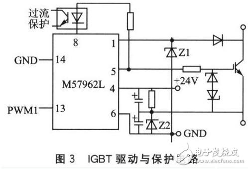
Figure 3 shows the principle of the drive circuit. The inverter device power device of the system adopts IGBT chip, so the drive circuit selects four drive modules M57962L produced by Mitsubishi Corporation. The drive module is a hybrid integrated circuit, which integrates the driving and overcurrent protection of the IGBT. In Figure 3, the 13th pin of the M57962L is connected to the PWM1 of the DSP (the other three M57962L are connected to PWM2, PWM3, and PWM4 respectively). The 14-pin grounding is connected to the power supply. In addition, the M57962L uses a low-voltage drive, which means that the M57962L can be driven only when the 13-pin input is negative. This has the advantage of preventing interference. When an interference waveform occurs, the M57962L with low-level drive cannot be driven. In addition, in the process of shutting down, if the voltage changes too much, it will cause the phenomenon of holding, causing the IGBT to run out of control, causing the upper and lower arms to pass through. Therefore, the RC snubber circuit is used to suppress the overvoltage and voltage change rate du/dt.
3, the digital implementation of the system
The system inverter part adopts the SPWM rule sampling algorithm. The basic idea is to change the output pulse according to the sine law, thus reducing the harmonic component in the output voltage and making the output voltage closer to the sine wave. In order to facilitate the digital implementation, the SPWM pulse sequence is generated by the regular sampling method, and the principle thereof is shown in FIG. Since the triangular carrier frequency is much higher than the sine wave frequency, the sinusoidal modulation wave ut in one cycle of the triangular carrier uc is regarded as constant, so that in a triangular wave cycle, only the sampling at point B is performed once, so that the generated SPWM can be generated. The midpoint of the pulse coincides with the midpoint of the corresponding triangular wave (point A), which greatly simplifies the calculation of the SPWM pulse. Let uc have an amplitude of 1, and the sinusoidal modulation signal ut = Msin ωtt, where O ≤ M "1 (M is the degree of modulation). Since △ABC~△EDA, there are:
The value of the sine function is obtained by looking up the table. In addition, N is a multiple of 3 in the synchronous modulation of each segment.
Software programming is the core of inverter control circuit design. The system software mainly includes: main program, interrupt service program, PI adjustment program, display program and the like. Figure 5 shows the main program flow, and Figure 6 shows the interrupt program flow. In the main program, complete DSP system and external device initialization, I/O control signal management and sine wave signal generation and processing. In the interrupt program, the current and voltage detection are completed, the PI adjustment calculation is performed, the modulation degree M and the frequency value under the constant voltage frequency ratio are calculated, the sine wave processing is performed, and the comparator CMPR1 is assigned.
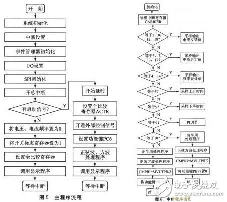
Figure 7 shows the PWM1 and PWM2 waveforms of the upper and lower tubes of the same bridge arm. It can be seen from the figure that the upper and lower arms are set with a dead time of 2 μs to ensure the safe operation of the inverter circuit. Figure 8 shows the PWM waveforms sent by the DSP. (1) and (2) are two complementary equal-width unequal-width pulse signals. The high level is +5 V, the low potential is OV, and the pulse width is changed according to the sine law. Since the M57962L chip uses a negative potential drive, a level shifter circuit is used. Figure 9 shows the SPWM waveform (converted SPWM waveform) of the final drive IGBT. As can be seen from the figure, the width of the waveform changes according to the sine law. Figures 10(a) and (b) show the output voltage waveforms at f = 200 Hz and f = 300 Hz, respectively. The experimental results show that the output voltage waveform quality is good and the total harmonic distortion rate is low.


in conclusion
DSP-based digital control technology can greatly improve product consistency, overcome product performance dispersion caused by analog control, enhance control flexibility, simplify system structure, and improve overall system stability and reliability. Good application prospects. This design application TMS320LF2407A chip uses SPWM control technology to complete the conversion of 380 V, 50 Hz AC power into an output AC 220V, frequency 100 ~ 400 Hz adjustable AC power. The actual measurement of the prototype shows that the output waveform quality is good, which overcomes the shortcomings such as large noise, slow response, and severe waveform distortion in the case of such a large-sized medium-frequency transformer, which is a product with good application prospects.
Black Light Tube,Blb Tube,Blb Bulb,Blb Lamp
Changxing leboom lighting product CO.Ltd. , https://www.leboomuv.com